
The Importance of PCB Layout
At EI Microcircuits, we do PCB layout for customers every day; let us help you with a few things we think will help you get the best results for a production-ready assembly.
A well-designed
printed circuit board (PCB) layout helps a circuit perform as intended while supporting reliable manufacturing, inspection, testing, and long-term operation. Component placement, routing, grounding, thermal paths, and spacing all influence how the finished board behaves after assembly.
A schematic defines how components connect, but the physical layout determines how electrical, thermal, and mechanical factors work together in production. Reviewing these decisions early reduces redesigns, identifies manufacturing constraints before production begins, and creates a stronger foundation for product reliability.
Why PCB Layout Matters Beyond Basic Routing
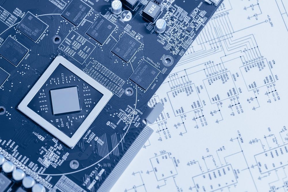
A PCB layout matters beyond basic routing because it determines how reliably a circuit performs and how efficiently it moves through manufacturing. While a schematic defines electrical connections, the physical arrangement of components, traces, planes, vias, and clearances influences signal quality, power distribution, thermal performance, manufacturability, inspection, testing, and long-term reliability. Effective PCB layout design balances these requirements before fabrication begins.
Every placement and routing decision creates downstream effects. Poor component spacing can complicate assembly, inadequate grounding can introduce electrical noise, and limited access to critical areas can make inspection and testing more difficult. Reviewing these factors early helps reduce redesigns, improve production efficiency, and create a stronger foundation for consistent product performance.
The Role of PCB Components in Layout Reliability
Every component placed on a circuit board introduces unique electrical, thermal, and mechanical considerations that influence the overall layout. Placement decisions affect signal paths, power distribution, heat dissipation, manufacturability, and testing. Understanding these relationships helps engineers create a layout that supports reliable performance while simplifying assembly and improving manufacturability.
Connectors
Connector locations establish many of the board's mechanical constraints. Early placement helps simplify cable routing, maintain structural integrity, provide adequate clearance, and ensure accessible connections during assembly, testing, and final product integration.
Capacitors
Capacitors should be placed as close as practical to the integrated circuits they support to stabilize voltage and minimize electrical noise. Careful placement also shortens current paths, improves power integrity, and reduces routing complexity throughout the board.
Relays
Relays often require additional board space because of their size and switching requirements. Their placement should account for high-current routing, electrical isolation, heat dissipation, and sufficient clearance to support reliable manufacturing and long-term operation.
Diodes
Diodes require correct orientation and adequate spacing to support reliable assembly and operation. Their placement should allow efficient routing while considering heat generation, polarity verification, and accessibility for inspection or replacement if servicing becomes necessary.
IC’s
IC’s frequently support high-density routing that demands careful planning for signal paths, power delivery, and thermal management. Positioning them with surrounding components in mind helps minimize congestion and creates a more manufacturable, reliable board layout.
Transistors
Transistors may generate significant heat depending on their application, making placement an important consideration. Providing sufficient spacing, appropriate copper areas, and efficient thermal paths supports reliable operation while simplifying assembly and long-term product performance.
Inductors
Inductors can introduce electromagnetic interference if placed too close to sensitive circuitry. Separating them from low-noise components and optimizing routing around magnetic fields helps improve signal quality while maintaining efficient power delivery throughout the design.
Resistors
Resistor placement influences trace length, signal accuracy, and heat distribution. Positioning resistors close to the circuits they serve can reduce unwanted electrical effects while maintaining accessible routing and adequate spacing for assembly, inspection, and future rework when required.
Integrated Circuits
Integrated circuits often determine the overall board layout because many surrounding components connect directly to them. Their placement influences routing efficiency, power distribution, thermal performance, and the available space needed for inspection, testing, and manufacturing processes.
Switches
Switch placement should balance electrical performance with user accessibility and mechanical design requirements. Proper positioning also supports efficient routing while maintaining the clearances needed for assembly, enclosure integration, and reliable operation throughout the service life.
Sensors
Sensor placement directly affects measurement accuracy because environmental conditions, electrical noise, and nearby heat sources can influence performance. Positioning sensors according to their operating requirements helps improve reliability while supporting efficient routing and manufacturability.
Signal Integrity, Power Delivery, and Grounding
Signal integrity, power delivery, and grounding work together to determine how reliably a circuit performs after assembly. Routing decisions, trace geometry, layer stack-up, and component placement all influence how signals travel across the board, how consistently power reaches components, and how effectively electrical noise is controlled. Designing these systems together helps minimize signal degradation, voltage fluctuations, crosstalk, and electromagnetic interference that can affect performance.
Grounding provides the stable return paths needed to support both signal integrity and power distribution. Continuous ground planes, controlled return paths, and proper separation between sensitive and high-power circuits help improve electrical stability while reducing noise. Addressing these considerations early creates a more reliable design, simplifies validation, and supports efficient manufacturing, inspection, and testing.
Thermal Management and Component Reliability
Effective thermal management helps maintain electrical performance while protecting components from excessive heat that can shorten service life or reduce reliability. Component placement, copper distribution, thermal vias, and airflow all influence how heat moves through a board during operation. Selecting the appropriate FR-4 material and board construction can also improve thermal stability for many applications, while higher-power designs may require specialized materials or additional cooling methods.
Thoughtful layout decisions help distribute heat more evenly, reducing hot spots that can accelerate component aging, increase solder joint stress, or affect long-term performance. Providing adequate spacing between heat-generating and temperature-sensitive components further improves reliability. Addressing thermal management early helps reduce design revisions, supports consistent manufacturing, and contributes to dependable operation throughout the service life.
How PCB Layout Affects Assembly, Inspection, and Testing
DFM (Design for Manufacturing), and DFT (Design for Test) are critical to the quality of your production-level device. EI Microcircuits does 100% DFM on every assembly that comes into our plant. We have a full Test Development team that will assist you in the DFT early in your design. They will also design a test process that meets the quality needs of your product, starting with a flying probe up through a full functional test.
PCB layout decisions continue to influence product quality long after fabrication is complete. Component spacing, orientation, clearances, and test point accessibility all affect assembly efficiency and process consistency. Thoughtful layout support automated component placement, reduces soldering challenges, and helps manufacturers meet
RoHS compliance requirements while minimizing production delays and costly rework.
Layout also determines how effectively a board can be verified throughout manufacturing and before shipment. Providing clear access to components, solder joints, and test points simplifies
PCB inspection and supports comprehensive
automated PCB test development throughout production. Depending on the application, manufacturers may use
flying probe testing to verify electrical connectivity without dedicated fixtures. Following a structured
PCB inspection checklist further helps identify defects early, improve product quality, and increase confidence that each assembled board meets design and manufacturing requirements.
Improving PCB Layout Outcomes Through Manufacturing Collaboration
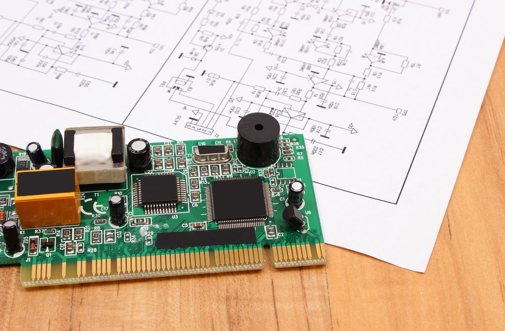
The best PCB layout results from early collaboration between design and manufacturing teams. Reviewing component placement, routing, thermal management, and test accessibility before fabrication helps identify potential production challenges while design changes remain practical to implement. This approach also supports downstream processes, including box-build integration and complete box-build assemblies.
At
EI Microcircuits, we help customers evaluate their PCB layout for manufacturability, testing, and long-term reliability before production begins.
Contact us to discuss your next PCB project and learn how EI Microcircuits can help optimize your layout for reliable, efficient manufacturing.


let's talk
EI Microcircuits is comprised of three production facilities totaling over 100,000 square feet of climate-controlled manufacturing, engineering and warehousing. We are ready to be the solution to your next project. Contact Us, Request a Quote or Schedule a Tour today!
Manufacturing plant 1
1651 Pohl Road
Mankato, MN 56001
P: 507.345.5786
Manufacturing plant 2
2011 Klein Street
St. Peter, MN 56082
P: 507.934.5722
manufacturing plant 3
69 Power Drive
Mankato, MN 56001
P: 507.386.9160
*Each facility is configured to support your production needs. While maintaining continuity with each other in equipment, training and process control, each facility offers its own specialty. All facilities share the same data center to allow for seamless manufacturing between locations.