


pcb engineering

EI Microcircuits is a solutions-driven partner specializing in advanced electronics. Our flexible project approach is tailored to each customer’s unique needs, with deep experience applied to optimize designs for layout, quality, and manufacturability. We support your product at every stage—from early design assistance through comprehensive DFM reviews—to help ensure a smooth path to production and long-term success.

full range project management

From concept to completion, our full-range project management ensures every PCB engineering phase is expertly coordinated, on time, and built to spec.

Red circuit diagram radiating from a central circle.

Project Management

Red circuit diagram radiating from a central circle.

Design for Manufacturing (DFM)

Red circuit diagram radiating from a central circle.

CAD Design

Red circuit diagram radiating from a central circle.

Alternate Component Sourcing

Red circuit diagram radiating from a central circle.

PCN (Part Changes Notifications) Management

Red circuit diagram radiating from a central circle.

EOL (End Of Life) Risk Evaluations

Red circuit diagram radiating from a central circle.

Stringent Records Control Necessary for Medical Devices

design for manufacturing

DFM Review

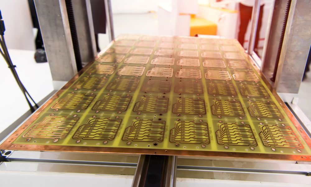
 EI’s DFM (design for manufacturability) process has a proven track record of product improvements and successful product launches. Project engineers perform DFMs incorporating years of experience and applying the latest software tools. Then our closed loop NPI process provides design feedback after the build.

highlighting altium

We leverage Altium’s advanced PCB design software to streamline layout, enhance accuracy, and ensure seamless integration from concept to production—empowering faster turnarounds and higher-quality builds.

Altium logo in bold, black sans-serif typeface.

Applications for PCB Engineering

EI Microcircuits engineers reliable, compliant PCB solutions for life-critical medical technologies and devices.

EI Microcircuits delivers durable, high-performance PCB assemblies built to withstand harsh industrial environments and continuous operation.

We design and manufacture robust PCB solutions that power critical energy systems with efficiency, accuracy, and long-term reliability.

From precision equipment to environmental monitoring, our PCBs support smarter, more sustainable agricultural technologies in the field.

EI Microcircuits builds high-layer count, high-performance assemblies for the emerging AI market. Our advanced SMT and quality systems ensure reliable, complex builds for HPC applications.

Our aviation-grade PCBs meet rigorous standards for performance, traceability, and safety in both commercial and defense flight systems.

Built for mission-critical use, our military-grade PCB solutions meet stringent durability and compliance requirements in high-demand environments.

We engineer secure, high-reliability PCBs for surveillance systems requiring real-time performance and dependable uptime.

our pcb engineering process

01.

Design Review

We collaborate early to review schematics and conduct Design for Manufacturability (DFM) analysis—ensuring your layout is optimized for efficient, high-yield production.

02.

Prototyping & Validation

Our rapid prototyping services turn designs into functional units fast, enabling thorough testing, feedback, and early design validation.

03.

Pre-Production Optimization

We fine-tune materials, processes, and test plans to ensure a smooth transition from prototype to full production—reducing risk and ensuring scalability.

04.

Full-Scale Production Support

With engineering oversight, quality control, and documentation throughout, we scale up seamlessly while maintaining precision and consistency across every unit.

our certifications

ISO 13485:2016 certified badge, AMTIVO logo, text "Medical Devices".
Logo for AMTIVO. ISO 9001:2015 Certified for Quality Management. Features a stylized "A".
A square badge with "AMTIVO" logo and "AS9100 D Certified Aerospace" text.
Blank white canvas.
White background.
Empty white background.

hear it from our customers

"A delightful company to work with. Could not have done it without your expertise."

"EI excels in responsiveness, support and flexibility. I very much appreciate EI’s ability to adapt on the fly."

"I appreciate the work EI does most of all because it makes my job easier."

"Overall, EI does a great job in dealing with everything we throw at them. They are responsive and understanding of us, even though it may not always be the most reasonable of requests. As a buyer, I feel lucky to have a supplier that works with us like they do."

"Working on a project that had a board that was simply not manufacturable the way it was set up, EI went above and beyond to help with engineering and still met a very short deadline."

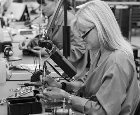
Two women in lab coats soldering components at a workbench.

PCB Engineering FAQs

  • What should be included in a PCB design for manufacturability review?

    A PCB design for manufacturability review should evaluate component footprints, spacing, polarity, solderability, panelization, thermal requirements, test access, and assembly constraints. We use DFM feedback to identify potential production risks before the design moves into manufacturing.

  • When should DFM be performed during PCB design?

    Complete DFM before releasing a design for production. Earlier collaboration gives engineering and manufacturing teams more opportunity to resolve component, layout, testability, and process concerns without creating unnecessary redesigns or schedule delays.

  • What PCB design files are needed for a manufacturing review?

    Provide the latest fabrication and assembly data, bill of materials, component placement information, drawings, test requirements, and applicable specifications. A complete release package helps us verify manufacturing intent and reduce engineering questions during new product introduction.

  • How can PCB engineering reduce manufacturing costs?

    PCB engineering can reduce total manufacturing cost by identifying difficult-to-source components, unnecessary process complexity, poor test access, assembly risks, and potential yield issues before production begins. The objective is a repeatable design rather than simply reducing individual component costs.

Electronic Insights

Gold-colored printed sheets on a large press machine in a workshop
August 26, 2026
Meta description: Learn how to navigate the PCB laminate shortage with DFM, material planning, and production strategies from EI Microcircuits.
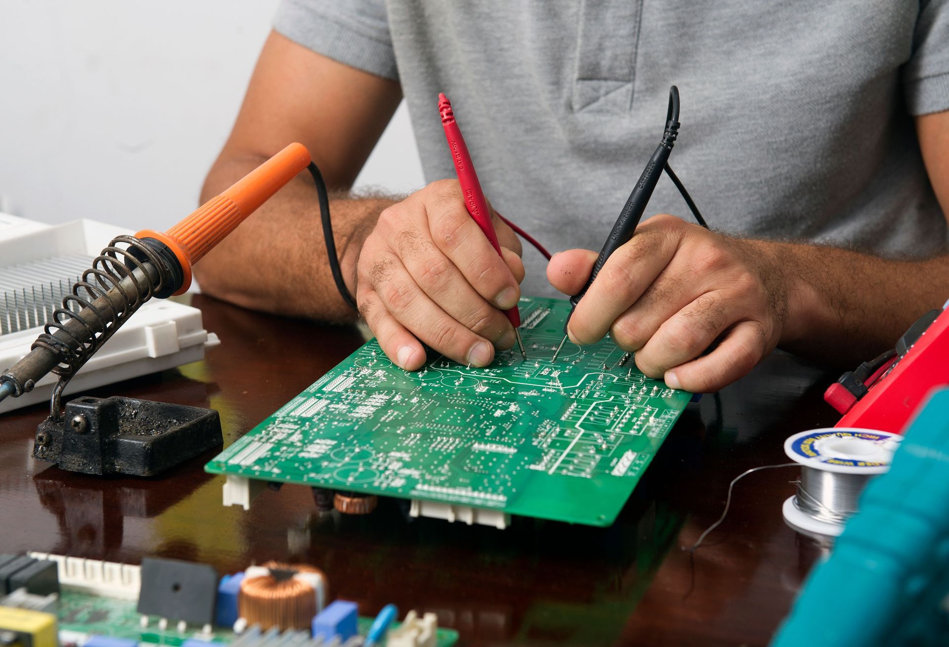
Person soldering a green circuit board on a workbench with tools nearby
August 21, 2026
PCB Material Selection impacts performance, reliability, and manufacturing. Learn key material considerations and applications with guidance from EI Microcircuits.
Blue circuit board overlaid on technical schematics with a central chip and small components
August 18, 2026
Learn how PCB layout impacts performance, manufacturability, testing, and long-term reliability with expert insights from EI Microcircuits.

let's talk

EI Microcircuits operates multiple climate-controlled facilities designed for scalability, technical excellence, and built-in disaster resilience—each fully equipped to support today’s most advanced electronic assemblies. Let us be the solution to your next project—Contact Us, Request a Quote, or Schedule a Tour today!

Contact Us Today

MANKATO, MN

1651 Pohl Road
Mankato, MN 56001

P:
 507.345.5786

ST. PETER, MN

2011 Klein Street
St. Peter, MN 56082

P:
 507.934.5722

MANKATO, MN

69 Power Drive
Mankato, MN 56001

P: 507.386.9160

*Each facility is configured to support your production needs. While maintaining continuity with each other in equipment, training and process control. All facilities share the same data center to allow for seamless manufacturing between locations.