What are PCB Pads?
Why PCB Pads Are Critical to Assembly Integrity
PCB pads define the connection points between components and the board, directly affecting solder joint formation, alignment, and electrical continuity. Poor pad layout can lead to issues such as insufficient wetting, bridging, or misalignment during assembly. These problems often result in rework, yield loss, or field failures. For high-reliability builds, pad geometry must match manufacturing capabilities to maintain consistent assembly performance and long-term product stability.
What Are PCB Pads?
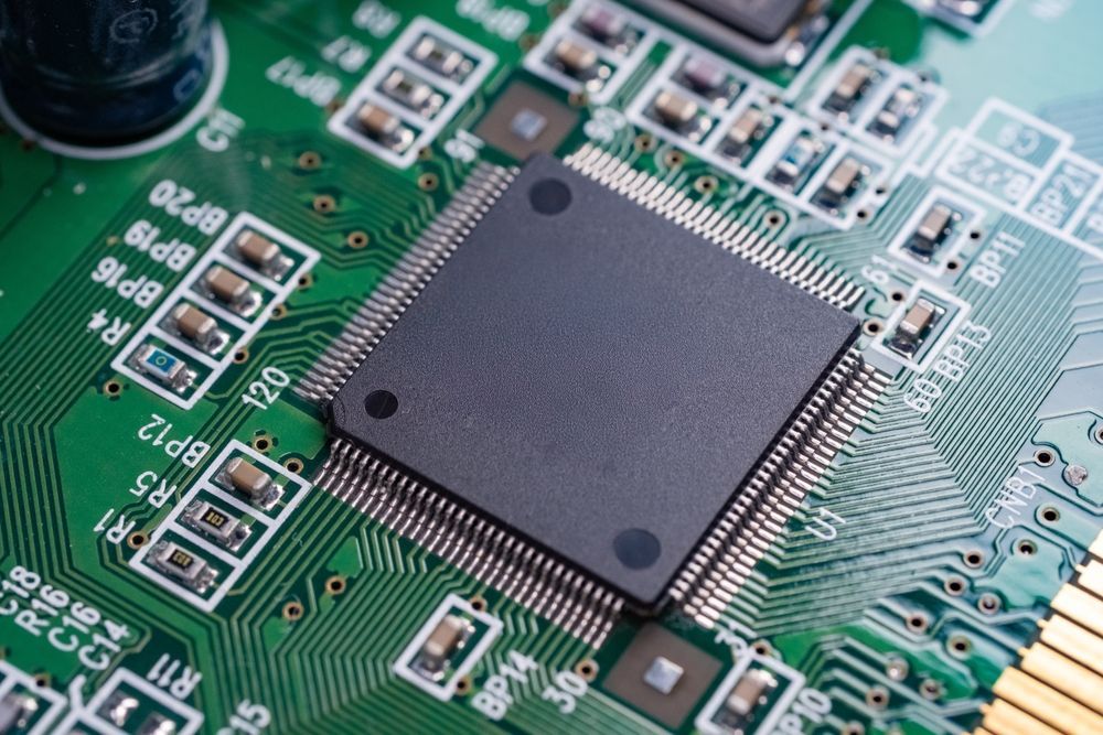
PCB pads are specific areas of exposed conductive material on a
printed circuit board (PCB) where component leads, or terminations, are mechanically secured and electrically connected. They form the interface between the board’s copper circuitry and the component, creating reliable solder joints during assembly. Pads are typically created by opening the solder mask to expose copper, followed by applying surface finishes that protect against oxidation and promote solderability. Their geometry, spacing, and surface condition must align with component requirements and assembly methods, since these factors directly influence connection strength, signal behavior, and durability across operating environments and applications.
Types of PCB Pads and Their Applications
PCB pad choice tracks closely with component style, assembly approach, and performance goals. The table below lists common pad types and their most common uses in both surface-mount technology (SMT) and through-hole designs.
| Pad Type | Application | Key Consideration |
|---|---|---|
| SMT Pads | Chip components, IC packages | Precise sizing for solder joint consistency |
| Through-Hole Pads | Connectors, mechanical components | Planted holes for structural strength |
| Thermal Pads | Power devices, heat-generating ICs | Heat dissipation and void control during reflow |
| Fiducial Pads | Board alignment for automated assembly | Optical clarity for accute placement systems |
Each pad type must correspond with assembly processes and inspection methods to maintain build quality and functional reliability.
Key Design Parameters for PCB Pads
When creating a PCB layout, pad geometry has to align with component data and assembly process limits. Small variations can influence solder behavior, placement accuracy, and long-term reliability.
Key parameters include:
Pad size and shape:
Match component land patterns to maintain consistent solder joints.
Spacing and pitch:
Prevent bridging and support accurate placement.
Solder mask clearance:
Define openings that balance protection and solder flow.
Surface finish choice:
Affects wettability, oxidation resistance, and shelf life.
Each factor must be evaluated within the broader manufacturing context to achieve repeatable assembly results and stable electrical performance.
Common PCB Pad Design Challenges
Pad-related issues often appear during assembly when design intent and process conditions diverge. Many challenges stem from material behavior, geometry, and interactions with solder masks.
Common issues include:
- Tombstoning: Uneven solder forces lift small components during reflow.
- Solder bridging: Excess solder or tight spacing creates unintended connections.
- Insufficient wetting: Poor surface finish or contamination limits solder adhesion.
- Pad misregistration: Misalignment between layers affects placement accuracy.
- Solder mask interference: Incorrect clearance restricts solder flow or exposes unwanted copper.
- Uneven copper distribution: Thermal imbalance influences solder flow and joint formation.
Each condition introduces variability that can affect yield, inspection results, and long-term assembly performance.
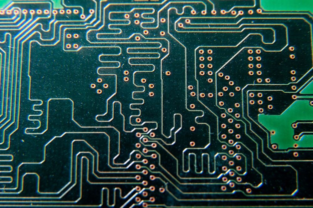
Manufacturing Implications of PCB Pads
Pad design choices influence how PCBs move through both fabrication and assembly. A clear understanding of how PCBs are made and how boards are manufactured highlights how pad geometry, plating, and surface finish interact with each step. During fabrication, pads must hold dimensional accuracy through etching and plating.
During assembly, they have to support consistent solder paste deposition and predictable reflow behavior. Inspection methods such as AOI and X-ray depend on distinct, repeatable pad features to find defects. When pad designs fall outside process capabilities, variability increases from build to build. Aligning pad specifications with manufacturing processes reduces rework, stabilizes yields, and strengthens overall assembly consistency.
PCB Pads in High-Reliability Applications
In high-reliability environments such as medical devices, aerospace systems, and defense electronics, pad performance has a direct impact on long-term product stability. These systems experience thermal cycling, vibration, and long service life expectations, which place additional stress on every solder joint. Pad design must account for material expansion rates, mechanical anchoring, and consistent electrical continuity across operating conditions.
Traceability and process control also become more demanding, with inspection methods focused on validating pad integrity throughout production. Small inconsistencies at the pad level can grow into larger system failures over time. Close coordination between pad design and controlled manufacturing processes contributes to predictable performance in demanding environments.
Advanced Considerations for Modern PCB Designs
As PCB layouts grow in density and complexity, pad design has to adapt to tighter tolerances and evolving component packages. High-density interconnect (HDI) layouts introduce smaller pads, finer pitches, and via-in-pad structures that call for precise fabrication control. Material choices play a greater role as thermal behavior and signal integrity become more sensitive to pad construction.
Newer packaging technologies, including BGAs and QFNs, put additional emphasis on pad uniformity and void control during reflow. These conditions call for alignment between design intent, fabrication capability, and inspection methods to maintain consistency across complex assemblies.
How EI Microcircuits Ensures PCB Pad Integrity
Within electronics manufacturing services (EMS), pad integrity depends on strong links between design data and controlled production processes. EI Microcircuits addresses this through early design-for-manufacturability reviews that focus on pad geometry, spacing, and material compatibility before production starts.
Our process uses inspection methods such as AOI, X-ray, and in-circuit testing to confirm solder joint formation and pad performance throughout assembly. Carefully managed process parameters, together with traceability systems aligned with quality management standards such as ISO 13485 and AS9100D, help keep results consistent across builds. This structured approach leads to repeatable outcomes for complex, high-reliability assemblies.
Precision at the Pad Level Drives Overall PCB Reliability
Pad-level choices shape outcomes across the entire assembly, influencing yield, inspection findings, and performance in the field. When these details match manufacturing processes, assemblies move through production more smoothly and with fewer disruptions. When they do not, small variations can eventually develop into more serious reliability issues.
For teams working on complex builds, early coordination between design and manufacturing often proves decisive. Partnering with an experienced EMS provider at this stage can clarify constraints and refine design details before production.
Connect with our team to review your design in a manufacturing context and explore practical ways to achieve stronger, more consistent assembly performance.

let's talk
EI Microcircuits is comprised of three production facilities totaling over 100,000 square feet of climate-controlled manufacturing, engineering and warehousing. We are ready to be the solution to your next project. Contact Us, Request a Quote or Schedule a Tour today!
Manufacturing plant 1
1651 Pohl Road
Mankato, MN 56001
P: 507.345.5786
Manufacturing plant 2
2011 Klein Street
St. Peter, MN 56082
P: 507.934.5722
manufacturing plant 3
69 Power Drive
Mankato, MN 56001
P: 507.386.9160
*Each facility is configured to support your production needs. While maintaining continuity with each other in equipment, training and process control, each facility offers its own specialty. All facilities share the same data center to allow for seamless manufacturing between locations.