Ultimate PCB Inspection Checklist
Behind every dependable electronic system is a disciplined inspection process. Printed circuit boards (PCBs) form the electrical foundation of nearly all modern devices, and even the smallest defect, like a weak solder joint, a misaligned component, or a contaminated surface, can compromise performance. In high-reliability industries such as medical, aerospace, and defense, the cost of one undetected flaw can extend far beyond a production line.
Types of PCB Inspections
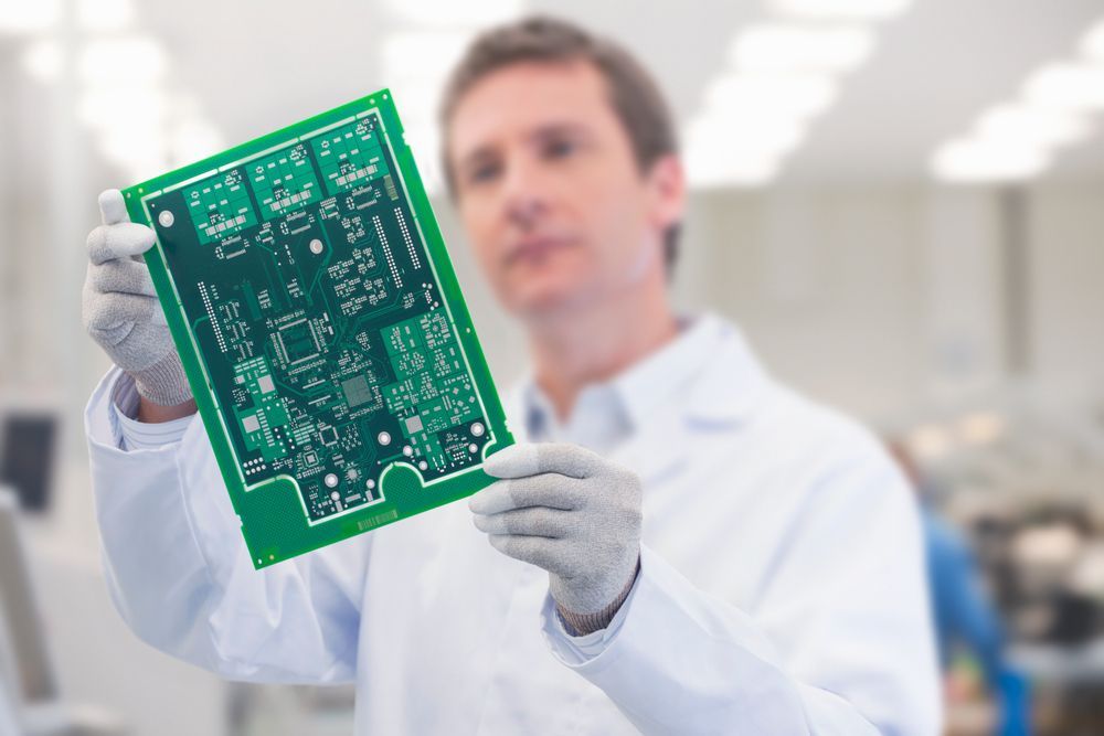
Visual and Manual Inspection
Manual inspection remains the first defense against obvious defects. Skilled technicians examine boards for visible issues such as solder bridges, missing parts, incorrect markings, and contamination. This step also verifies alignment and assembly cleanliness, especially useful during early builds or low-volume production where automated systems may not yet be configured.
Automated Optical Inspection (AOI)
AOI systems use high-resolution cameras and pattern-recognition software to compare every solder joint and component against the digital reference design. AOI identifies polarity errors, insufficient solder, and lifted leads faster and more accurately than the human eye. For surface mount assemblies, it provides a repeatable, objective check early in the process. And all of this occurs before boards move to test or final assembly.
X-ray Inspection (AXI)
X-ray inspection penetrates components and solder joints, allowing technicians to evaluate connections hidden beneath packages such as BGAs, QFNs, and LGAs. It reveals voiding, bridging, or insufficient solder volume that cannot be seen visually. AXI is particularly vital in fine-pitch assemblies and high-density interconnects, where unseen defects can impact both signal integrity and mechanical reliability.
In-Circuit Testing (ICT)
ICT applies a bed-of-nails fixture to verify electrical continuity, component values, and correct circuit operation. It checks for shorts, opens, and out-of-tolerance components at the net level. ICT is efficient for stable, high-volume production where repeatability and speed are priorities.
Flying Probe Testing (FPT)
Flying probe systems perform similar electrical checks to ICT without the need for custom fixtures. They use movable test probes to contact pads, vias, and test points directly. This method is ideal for prototypes or low-volume runs where changes occur frequently and test flexibility is critical.
Functional Testing (FCT)
Functional testing simulates real-world operation. It confirms that the assembled board performs according to its intended function under controlled conditions. Parameters such as voltage, current, and signal behavior are measured while the board interacts with its supporting systems or test harness. Functional tests serve as the final proof that every preceding process produced a stable, working assembly.
Pre-Inspection Considerations
Effective inspection starts with preparation. Before testing begins, boards must be fully cured, cleaned, and labeled. Inspection criteria should align with customer specifications and IPC standards such as IPC-A-610 and IPC-6012.
Environmental factors, like lighting, magnification, and ESD control, should also be verified to prevent accidental contamination or handling damage during evaluation. Finally, inspection documentation and checklists should be approved and traceable to each production batch, establishing a clear quality record for future audits.
Core PCB Inspection Checklist
A structured inspection checklist ensures consistency across teams, builds, and product lines.
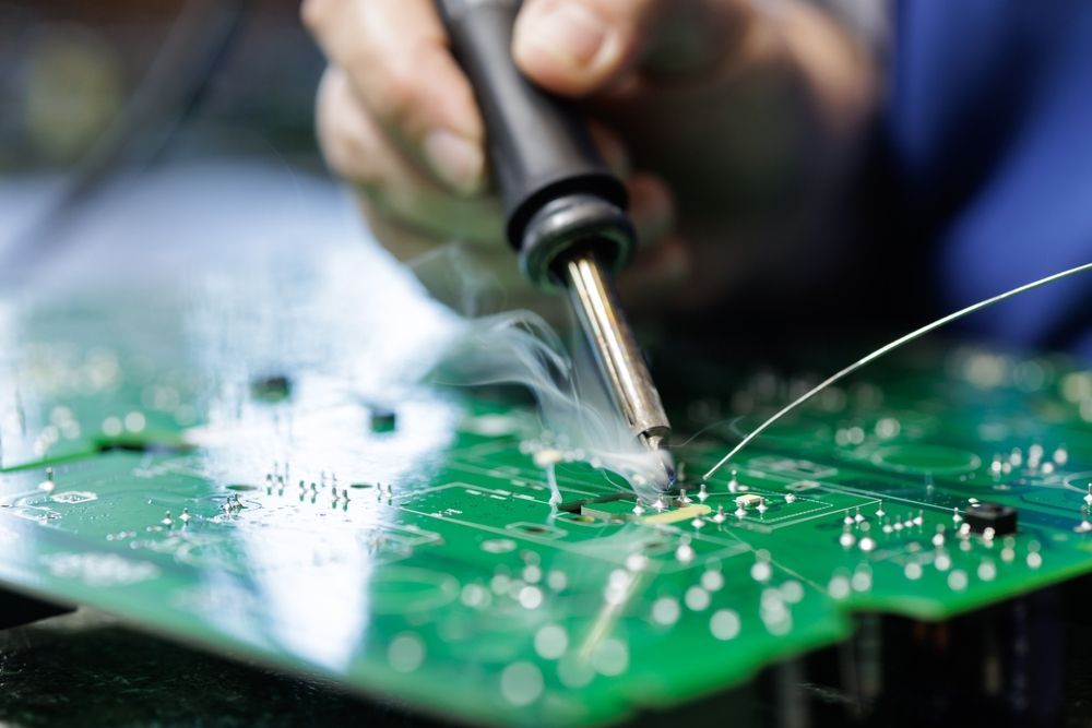
Solder Joint Quality
- Verify uniform wetting, correct fillet shape, and absence of voids or bridges.
- Check for dull, grainy, or cracked joints that may indicate cold solder or contamination.
- Inspect for excessive solder that could cause shorts or mechanical stress.
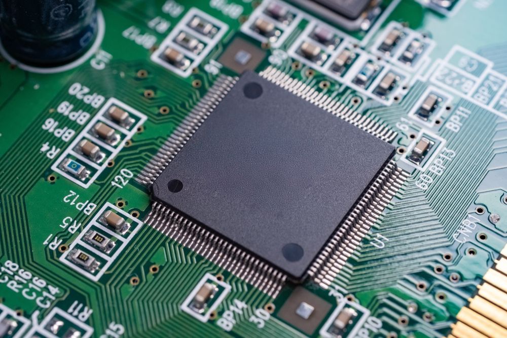
Component Placement and Orientation
- Confirm alignment to pads, especially for fine-pitch and polarized components.
- Validate that all part numbers match the bill of materials (BOM).
- Check for tombstoned resistors, lifted leads, or skewed parts caused by reflow imbalance.
Solder Mask and Silkscreen Accuracy
- Ensure that solder mask openings align with pads and vias, preventing solder bridging.
- Confirm legible, accurate silkscreen markings for reference designators and polarity.
- Check for mask bleed, voids, or contamination that could affect assembly or rework.
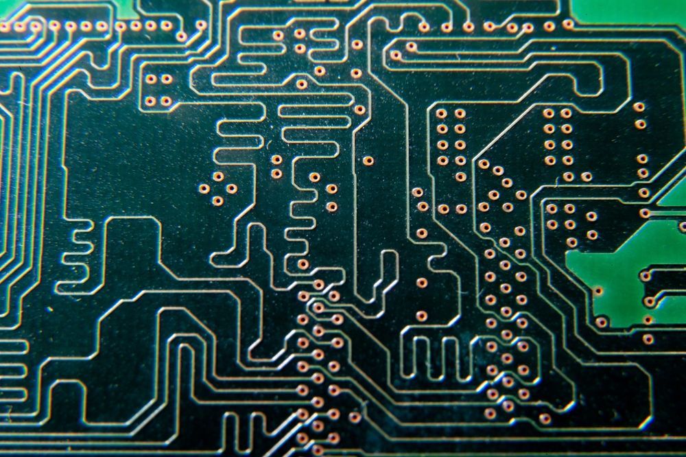
Trace Integrity and Pad Damage
- Inspect traces for nicks, cuts, or over-etching.
- Verify pad adhesion and copper thickness in high-current areas.
- Check for damage near connectors or plated through-holes that may weaken the circuit.
Cleanliness and Foreign Object Debris (FOD)
- Examine surfaces for flux residue, dust, fibers, or metallic debris.
- Confirm ionic contamination is within limits per IPC J-STD-001.
- Verify cleaning methods and solvents have not damaged coating or markings.
Conformal Coating and Overmolding
- Ensure uniform coverage, correct thickness, and full cure without bubbles or peeling.
- Verify masking accuracy, which means no coating on connectors, test points, or contact pads.
- Inspect overmolded assemblies for voids or incomplete encapsulation that could trap moisture or compromise flexibility.
Mechanical Integrity
- Check board flatness, connector alignment, and mounting hole accuracy.
- Inspect standoffs, fasteners, and mechanical supports for torque and fit.
- Confirm assemblies meet defined tolerances for insertion force and dimensional stability.
Compliance and Documentation
Inspection is the safeguard to identify defects and prove compliance. Each verification point must be recorded with lot codes, inspection dates, and operator sign-offs. Visual data, such as AOI or X-ray images, should be archived for traceability.
For regulated industries, documentation must link inspection results to material batches, calibration records, and final acceptance criteria. At EI Microcircuits, inspection data is digitally logged and integrated into our manufacturing execution system (MES), ensuring full visibility from incoming material to outgoing shipment.
Common Inspection Pitfalls to Avoid
Even experienced teams can overlook subtle risks during inspection. Common issues include:
- Relying solely on visual inspection for hidden defects.
- Skipping intermediate AOI checks between SMT and final assembly.
- Failing to recalibrate test equipment or update test programs after engineering changes.
- Inconsistent documentation across production shifts or facilities.
Avoiding these pitfalls requires both process discipline and cross-team communication. And inspection should never function as an isolated task, because it’s part of a continuous quality loop that includes design, assembly, and corrective action feedback.
How EI Microcircuits Ensures Inspection Excellence
At EI Microcircuits, inspection is embedded into every phase of production. Each assembly moves through defined verification stages supported by advanced inspection technologies, experienced technicians, and closed-loop process control.
- AOI and X-ray verification confirm solder integrity for all SMT and through-hole builds.
- Flying probe and ICT testing validate continuity and circuit function before integration.
- Functional testing and environmental stress screening replicate real-world conditions to verify performance over time.
All inspection data is logged and traceable through our quality management systems that are
certified to ISO 9001, ISO 13485, and AS9100D. Our documentation protocols support full audit readiness for all our customers, including medical, aerospace, and defense.
Expect Solutions at Every Stage
Every engineer knows what’s at risk when a defect escapes detection. One weak solder joint can trigger field failures, one trace break can halt production, and one missing record can stall certification.
At EI Microcircuits, we help teams turn inspection from a reaction into a strategy by using disciplined processes, advanced inspection tools, and transparent reporting to reinforce quality from the inside out. Our engineers work alongside yours to review designs, validate inspection criteria, and apply the right technology for every build. Our production and QA teams ensure every board meets the specifications it was designed for, and every audit standard it will face.
Partner with EI Microcircuits for PCB manufacturing and inspection systems engineered to eliminate risk, enhance traceability, and deliver performance that endures. Together, we’ll make precision a guarantee, not a goal.
let's talk
EI Microcircuits is comprised of three production facilities totaling over 100,000 square feet of climate-controlled manufacturing, engineering and warehousing. We are ready to be the solution to your next project. Contact Us, Request a Quote or Schedule a Tour today!
Manufacturing plant 1
1651 Pohl Road
Mankato, MN 56001
P: 507.345.5786
Manufacturing plant 2
2011 Klein Street
St. Peter, MN 56082
P: 507.934.5722
manufacturing plant 3
69 Power Drive
Mankato, MN 56001
P: 507.386.9160
*Each facility is configured to support your production needs. While maintaining continuity with each other in equipment, training and process control, each facility offers its own specialty. All facilities share the same data center to allow for seamless manufacturing between locations.