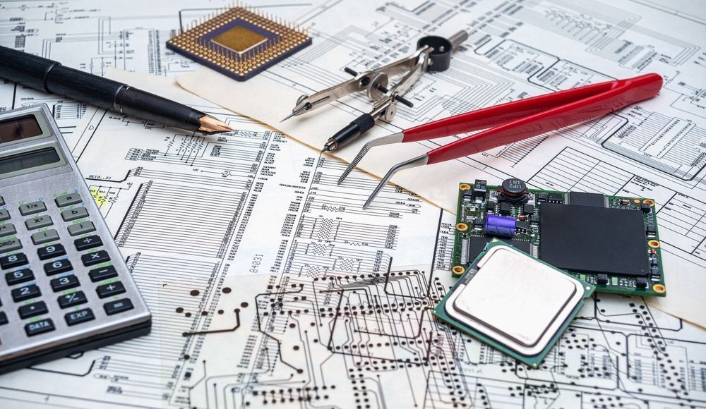
How to Design a PCB Layout
Every electronic device, from implantable monitors to avionics systems, starts with layout decisions that shape reliability, performance, and manufacturability.
PCB layout design influences signal behavior, thermal balance, and solder quality. Though often treated as a late-stage task, early alignment between layout and system goals improves production flow and long-term consistency.
Understanding the Design Process
PCB layout design works best when treated as part of an integrated development flow, not an isolated task after schematic capture. Each step, including requirements gathering, component selection, placement, routing, review, and release, builds on the one before it.
Gaps in coordination between electrical, mechanical, and manufacturing teams often result in costly late-stage changes. Misalignment at any point can delay schedules, increase revision cycles, and introduce downstream risk.
A structured process connects design intent to physical implementation, aligning layout goals with system constraints. Early collaboration across disciplines helps avoid rework, supports compliance with industry standards, and lays the foundation for reliable
production outcomes.
Define the Requirements
A strong PCB layout starts with a clear understanding of performance, regulatory, and environmental conditions. Electrical specifications such as voltage ranges, current loads, impedance targets, and timing constraints shape placement and routing.
Mechanical boundaries, connector locations, and enclosure dimensions define the board outline and layer count. For regulated sectors, documentation must reflect traceability and follow applicable standards like IPC-2221 or IPC class certifications required for medical and aerospace builds.
Capturing these inputs early minimizes design churn and improves coordination between disciplines. Clarity at this stage drives better build quality and long-term reliability.
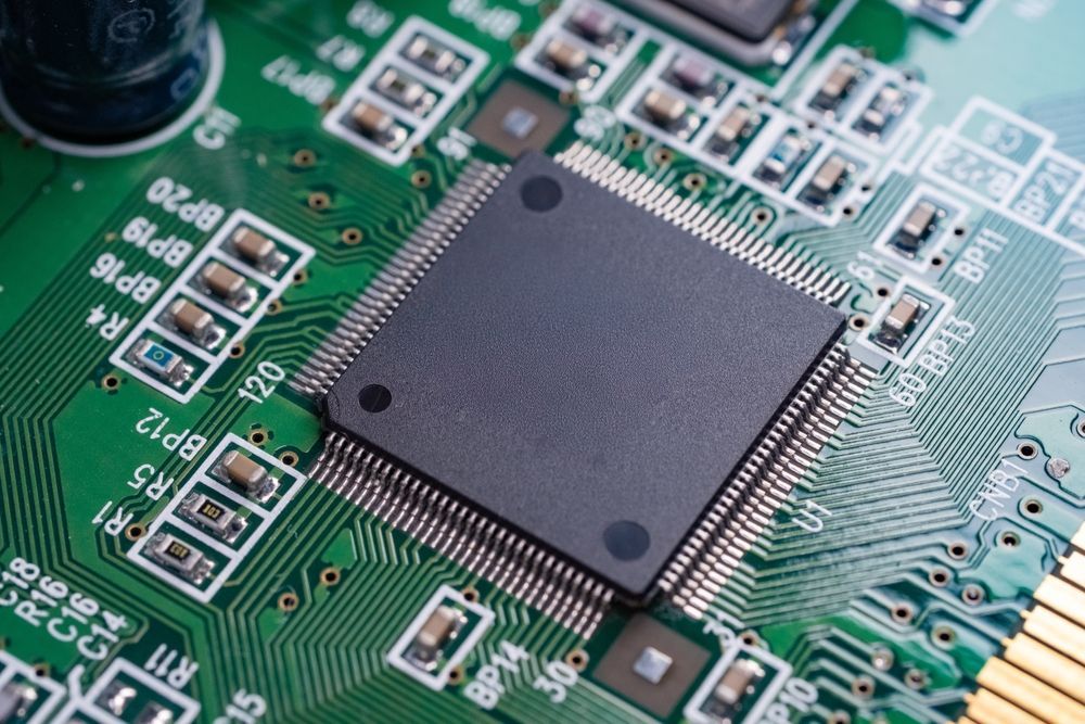
Component Placement Strategy
Placement defines the electrical, thermal, and mechanical performance of the finished assembly. Early decisions here can reduce trace complexity, protect signal integrity, and shorten routing paths. Functional grouping and clear zoning help maintain performance and streamline inspection.
Key considerations include:
- Keep decoupling capacitors close to IC power pins
- Orient polarized components consistently to ease inspection
- Separate analog and digital sections to limit interference
- Reserve edge space for connectors and mounting hardware
- Maintain clearance for test points and probe access
- Optimize the location of through-hole assemblies for structural stability and clean soldering
Signal Routing Fundamentals
Effective signal routing balances electrical performance with layout constraints. Trace width, spacing, and path length all affect impedance, crosstalk, and timing. High-speed signals benefit from direct paths and controlled impedance, while differential pairs require consistent spacing.
Avoid right-angle turns to limit signal reflection. Minimize via use to preserve signal quality. Power and ground planes should remain continuous and clean to maintain low-impedance return paths.
Routing choices made at this stage influence EMI behavior, manufacturability, and stability during test and final use.
Design for Manufacturability (DFM) Best Practices
Designing for manufacturability reduces delays, prevents defects, and promotes consistent yield. Layout choices should account for spacing, component orientation, thermal relief, and silkscreen clarity. Collaboration with manufacturing partners early in layout stages strengthens alignment between design and production.
Common DFM practices include:
- Maintain copper-to-edge clearance to avoid panelization issues
- Use consistent component orientation to assist automated placement
- Allow proper spacing for solder joints, reflow, and cleaning
- Avoid placing vias in pads unless using via-in-pad techniques
- Include fiducials and tooling holes for alignment and handling
- Create solder mask openings to prevent bridging and ensure coverage
Design for Testability (DFT)
Testability begins during layout, not after production. Without access to key nets or proper probe points, testing becomes time-consuming and incomplete.
Routing should accommodate fixture access, provide spacing for test pads, and isolate key circuits to enhance fault detection. For boundary scan or flying probe methods, test access must be consistent and unobstructed.
Solid DFT practices reduce debug time, raise fault coverage, and reinforce consistent quality control, especially in regulated or high-reliability applications.
Materials, Stack-Up, and Layer Management
Material selection and layer configuration shape how the PCB handles signal speed, power delivery, and thermal behavior. While FR4 remains standard, specialized substrates may be required for high-speed or elevated temperature environments.
Layer stack-up impacts impedance control, EMI shielding, and crosstalk. Balanced layers reduce warping and enhance fabrication. Power and ground planes must be planned to support clean return paths and stable voltages.
In dense designs, careful stack-up planning helps avoid redesigns and aligns with both regulatory and technical standards. A well-defined layer plan also streamlines fabrication and improves lot-to-lot consistency.
Tools and Standards to Follow
Reliable PCB layout design depends on using validated tools and following industry-recognized standards. These guide how footprints are created, how design rules are enforced, and how files are prepared for manufacturing. Consistency in tools and standards reduces errors and supports traceability across revisions and builds.
Commonly used tools:
- Altium Designer
- KiCad
- OrCAD / Cadence Allegro
- Mentor Graphics PADS
- Autodesk Eagle
Standards frequently applied in layout design:
- IPC-2221 for generic PCB design
- IPC-7351 for land pattern design
- ISO 13485 or AS9100D for regulated industries
- ANSI ESD S20.20 for electrostatic discharge control
- Manufacturer-specific handling rules for SMT technology
Preparing for Fabrication
Once the layout is finalized, preparing for fabrication involves more than exporting Gerber files. The documentation package should include fabrication drawings, drill files, netlists, and a clean bill of materials.
Details such as stack-up, impedance specs, and finish notes, such as soldermask or coating, must be clearly documented. Consistent file naming and revision tracking lower the risk of production delays.
When design intent is accurately translated into manufacturing data, it improves yield, speeds up first-pass success, and strengthens the relationship between
engineering and production teams.
Closing the Loop with Lifecycle Support

A well-executed layout supports consistent builds and carries value throughout the product’s lifecycle. Design decisions made upfront influence serviceability, product updates, and field reliability.
Working with a manufacturing partner that handles layout input, testing, box builds, and revisions reduces internal strain and simplifies supplier management. This level of continuity supports fewer disruptions and steadier production over time.
Contact us to learn how EI Microcircuits manages full-lifecycle electronics manufacturing for high-reliability applications, including
surface mount assembly (SMT), box-build integration, and traceable test coverage.


let's talk
EI Microcircuits is comprised of three production facilities totaling over 100,000 square feet of climate-controlled manufacturing, engineering and warehousing. We are ready to be the solution to your next project. Contact Us, Request a Quote or Schedule a Tour today!
Manufacturing plant 1
1651 Pohl Road
Mankato, MN 56001
P: 507.345.5786
Manufacturing plant 2
2011 Klein Street
St. Peter, MN 56082
P: 507.934.5722
manufacturing plant 3
69 Power Drive
Mankato, MN 56001
P: 507.386.9160
*Each facility is configured to support your production needs. While maintaining continuity with each other in equipment, training and process control, each facility offers its own specialty. All facilities share the same data center to allow for seamless manufacturing between locations.