
PCB History: From Early Circuits to Modern Manufacturing
PCB history began with printed-circuit concepts in the early 1900s and progressed through wartime electronics, commercial radios and televisions, multilayer boards, surface-mount technology, and today’s high-density assemblies. Over time, printed circuit boards replaced complex point-to-point wiring with more compact and repeatable methods for connecting electronic components.
Each advance also changed manufacturing. Greater circuit density led to more sophisticated board construction, assembly, inspection, and testing processes. Today, DFM, AOI, X-ray, ICT, functional testing, and disciplined process controls reflect more than a century of progress toward reliable, repeatable electronics production.
Early 1900s–1930s: The Origins of Printed Circuits
The foundations of
printed circuit boards (PCBs) emerged as inventors searched for more practical ways to connect electrical components. Early electronics relied heavily on individual wires and point-to-point connections, which became harder to manage as circuits grew more complex. Between the early 1900s and 1930s, new concepts for placing conductive paths onto insulating materials began shaping the construction methods that later became standard.
Early PCB Concepts and Patents
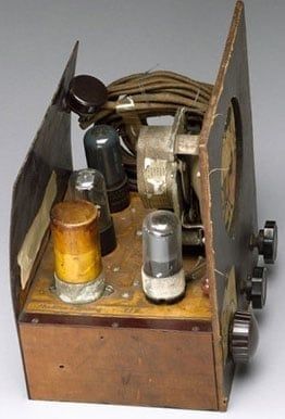
Several inventors contributed ideas that eventually shaped modern circuit board construction. In 1903, German inventor Albert Hanson filed a patent describing flat foil conductors laminated to an insulating material in multiple layers. His concept anticipated features later associated with multilayer board construction. During the 1920s, American inventor Charles Ducas developed another important concept by proposing conductive paths applied directly to an insulated surface.
These early patents did not immediately lead to widespread commercial production. Manufacturing methods, materials, and electronic components still needed to advance before printed circuits could replace conventional wiring on a large scale. Still, the concepts established an important principle: electrical connections could be incorporated into a structured substrate rather than created entirely from individual wires between components.
Radios and the First Practical Printed Circuits
Radio technology helped move printed circuits closer to practical use. Austrian engineer Paul Eisler developed an etched-foil printed circuit while working with radio electronics during the 1930s and 1940s. His approach used conductive copper foil bonded to an insulating base, with unwanted copper removed to leave the intended circuit pattern. This method more closely resembles later subtractive PCB fabrication techniques.
Printed circuits still faced barriers to broad adoption. Point-to-point wiring was already established, and early production methods did not yet have the automation, materials, or process consistency associated with later PCB manufacturing. Radios nonetheless demonstrated how printed conductors could reduce complicated wiring arrangements and create a more repeatable path toward assembling increasingly complex electronic products.
1940s: World War II Accelerates PCB Development
World War II increased the need for electronics that could be produced consistently for communications, navigation, and other military systems. Printed-circuit techniques gained attention as manufacturers searched for alternatives to labor-intensive wiring methods. During this period, Paul Eisler continued advancing printed-circuit methods, while wartime applications demonstrated the value of more standardized electrical connections.
The decade also helped establish techniques suited to higher-volume production. As electronics became increasingly important to military operations, manufacturers needed dependable methods for assembling circuits with fewer manual wiring steps. These developments created a foundation for broader commercial adoption after the war, when printed circuits began moving into consumer and industrial electronics.
PCBs in Military and Communications Equipment
Military communications equipment placed a premium on compact construction, repeatability, and dependable electrical connections. Radios, proximity fuzes, radar-related equipment, and other wartime electronics contained growing numbers of components, increasing the difficulty of assembling complex circuits entirely through point-to-point wiring.
Printed-circuit techniques helped manufacturers create standardized conductive paths that could be reproduced across multiple units. One significant wartime application involved proximity fuzes, where printed circuits contributed to compact electronic assemblies produced in large quantities. The U.S. military’s use of printed-circuit technology during and after the war also helped advance manufacturing methods and broader acceptance.
The significance extended beyond individual military products. Wartime production demonstrated that printed circuitry could address practical manufacturing problems at scale. Those lessons carried into postwar electronics as manufacturers applied similar principles to communications equipment and expanding commercial markets.
1950s–1960s: PCBs Enter Mainstream Electronics
During the 1950s and 1960s, printed circuitry moved from specialized applications into broader commercial production. Manufacturers adopted more standardized fabrication methods as consumer electronics expanded and electronic systems became increasingly complex. Through-hole construction became common, with component leads inserted into drilled holes and soldered to conductive features on the board.
Industry standardization advanced alongside these manufacturing methods. IPC formed in 1957 as printed wiring developed into a growing industry. More consistent specifications for materials, dimensions, workmanship, and board construction helped manufacturers produce assemblies with greater repeatability as electronics entered homes, businesses, and computing environments. Standardized acceptance criteria also established a common framework for evaluating workmanship as PCB production expanded.
PCBs in Radios, Televisions, and Early Computers
Consumer electronics helped turn circuit boards into a mainstream manufacturing technology. Radios and televisions were produced in increasing quantities, creating a strong incentive to replace extensive hand wiring with standardized board assemblies. Circuit boards simplified component placement and electrical interconnections while creating more consistent production processes across repeated builds.
Computers presented another challenge. As systems incorporated more transistors and, later, integrated circuits, designers needed practical methods for organizing a growing number of electrical connections. Circuit boards became central to connecting processors, memory, and supporting components within these systems.
The introduction of integrated circuits during this period further increased functional density. More circuitry could occupy less physical space, setting the stage for denser layouts, multilayer construction, and new component-mounting methods in the decades that followed.
1970s–1980s: Smaller, More Complex Circuit Boards
Electronics advanced rapidly during the 1970s and 1980s as integrated circuits placed more functions into increasingly compact packages. Circuit boards had to accommodate higher connection counts without excessive growth in physical size. Manufacturers responded with finer conductive features, additional board layers, and increasingly automated assembly processes. This stage of PCB history helped establish the manufacturing foundation for personal computers, telecommunications systems, and sophisticated industrial equipment.
Multilayer Boards and the Rise of Surface Mount Technology
Multilayer construction became increasingly valuable as circuit complexity exceeded the practical routing capacity of single- and double-sided boards. By stacking conductive layers separated by insulating materials, designers gained additional space for signal routing, power distribution, and grounding while maintaining manageable board dimensions. Connections between layers could be established through plated holes and vias.
Surface-mount technology also gained momentum during the 1980s. Instead of inserting component leads through drilled holes, manufacturers could place many components directly onto pads on the board surface. Smaller packages and shorter connections contributed to greater component density and more compact assemblies. SMT also aligned well with automated placement and soldering processes. Together, multilayer construction and surface mounting created new options for increasingly sophisticated electronics while raising expectations for fabrication precision and assembly process control.
PCBs in Computers, Telecommunications, and Industrial Equipment
The growth of personal computing and telecommunications accelerated the need for boards capable of carrying more components and connections within limited spaces. Computers relied on increasingly complex assemblies for processing, memory, storage interfaces, and peripheral functions. Telecommunications equipment faced similar pressures as networks expanded and electronic switching systems became more sophisticated.
Industrial applications also benefited from advances in PCB construction. Control systems, instrumentation, motor controls, and factory equipment increasingly incorporated electronic assemblies to manage operations and monitor processes. These applications introduced practical concerns beyond component density, including long service lives, repeatable production, and operation under challenging environmental conditions.
By the end of the 1980s, circuit boards had become foundational across numerous electronic product categories. Greater complexity also set the stage for tighter manufacturing controls and more advanced inspection methods in subsequent decades.
1990s–Today: High-Density, High-Reliability PCBs
Since the 1990s, PCB development has centered on greater circuit density, smaller components, and tighter manufacturing tolerances. High-density interconnect technologies and advanced component packages have expanded design possibilities while increasing fabrication and assembly complexity. Manufacturing practices have also adapted to requirements such as RoHS compliance, which restricts certain hazardous substances in electrical and electronic products. These changes place greater emphasis on controlled, repeatable production processes.
Miniaturization, Advanced Components, and Higher Circuit Density
Modern electronics place substantial functionality into increasingly compact assemblies. Fine-pitch components, BGAs, QFNs, microvias, and high-density interconnect structures help designers increase connection density while controlling overall board size. These technologies are common in products where space, weight, performance, and reliability influence design decisions.
Greater density also introduces manufacturing challenges. Smaller pads and tighter component spacing reduce process margins, while solder joints beneath BGAs and QFNs cannot be fully evaluated through conventional visual inspection. Precise placement, controlled soldering processes, and appropriate inspection methods become increasingly important as designs grow more complex. For OEM teams, these factors place greater emphasis on evaluating manufacturability early and selecting assembly and inspection processes suited to the board design, component packages, production volume, and end-use requirements.
Medical, Aerospace, Defense, and Industrial Applications
High-reliability electronics serve applications where assembly performance, process control, and traceability carry significant consequences. Medical electronics can involve stringent quality requirements and detailed production records for assemblies used in diagnostic, monitoring, and treatment equipment. Aerospace and military programs often place additional emphasis on reliability, configuration control, and consistent workmanship for electronics exposed to demanding operating conditions.
Industrial electronics present their own manufacturing considerations. Automation controls, sensors, instrumentation, and other equipment may operate for extended periods in environments affected by temperature, vibration, moisture, or contaminants. Across these sectors, increasing PCB complexity has strengthened the role of documented processes, appropriate inspection, electrical testing, and traceability. Manufacturing strategies must align board design and production controls with the reliability expectations and operating conditions of the finished product.
How PCB Manufacturing and Testing Have Evolved
As circuit boards became denser and component packages became smaller, manufacturing and testing processes advanced alongside them. Automated placement, controlled solder paste application, reflow profiling, and process monitoring increased consistency across complex assemblies. Inspection also expanded beyond manual visual checks as connections became smaller or hidden beneath components.
Modern production uses multiple inspection and test methods because each addresses different characteristics. DFM reviews can identify manufacturability concerns before production, while automated inspection and electrical testing evaluate assemblies at later stages. Together, these processes help manufacturers identify defects, verify workmanship, assess electrical performance, and maintain repeatability across production runs. Earlier identification can also limit rework and production delays while reducing the risk of defects reaching later assembly stages.
DFM, AOI, X-Ray, ICT, and Functional Testing
Modern inspection and testing begin before components reach the assembly line. Design for manufacturability (DFM) reviews identify concerns involving component placement, spacing, materials, and assembly processes before production. During assembly, automated optical inspection (AOI) can detect visible defects such as component misalignment and soldering anomalies. X-ray inspection examines connections hidden beneath packages such as BGAs and QFNs.
Electrical methods address different risks. In-circuit testing (ICT) can check individual components and circuit connections, while functional testing evaluates assembly operation under defined conditions. When failures occur, structured
PCB troubleshooting can help isolate defects and determine appropriate corrective action. Using complementary inspection and test methods gives manufacturing teams greater visibility into workmanship and electrical performance while reducing the risk of defects progressing into later production stages.

How EI Microcircuits Supports Modern PCB Assembly
EI Microcircuits applies modern manufacturing controls across high-mix, low- to medium-volume electronics programs. Capabilities include surface-mount and through-hole assembly, AOI, X-ray inspection, flying probe, ICT, functional testing, conformal coating, overmolding, and box-build integration.
For OEM teams, coordinating these processes through one manufacturing partner can simplify supplier management while maintaining continuity from PCBA through final assembly. Continuity across engineering feedback, material management, assembly, testing, and final integration can also strengthen consistency across production runs. EI Microcircuits also incorporates DFM consultation and a closed-loop NPI process to identify manufacturing concerns early. Quality management systems such as ISO 13485 and AS9100D further align manufacturing controls with high-reliability medical and aerospace programs. This approach is especially relevant for high-reliability programs where traceability, process consistency, flexible production, and lifecycle manufacturing remain important from initial builds through ongoing production.
What the History of PCBs Tells Us About Their Future
The PCB history timeline shows a consistent progression toward greater density, precision, and manufacturing control. Future advances will continue pushing component packaging, board construction, inspection, and testing processes as electronic systems become more complex.
For OEM teams, a practical path is clear: review manufacturability early, align production and testing methods with application requirements, and select a manufacturing partner prepared for the product lifecycle. Strong process control can reduce production risk while maintaining consistency as programs evolve. Ready to discuss a high-reliability electronics program?
Contact us to talk with EI Microcircuits about the manufacturing challenges behind the design.
let's talk
EI Microcircuits is comprised of three production facilities totaling over 100,000 square feet of climate-controlled manufacturing, engineering and warehousing. We are ready to be the solution to your next project. Contact Us, Request a Quote or Schedule a Tour today!
Manufacturing plant 1
1651 Pohl Road
Mankato, MN 56001
P: 507.345.5786
Manufacturing plant 2
2011 Klein Street
St. Peter, MN 56082
P: 507.934.5722
manufacturing plant 3
69 Power Drive
Mankato, MN 56001
P: 507.386.9160
*Each facility is configured to support your production needs. While maintaining continuity with each other in equipment, training and process control, each facility offers its own specialty. All facilities share the same data center to allow for seamless manufacturing between locations.