
Explaining PCB Lamination
A multilayer circuit board can pass initial inspection yet develop problems after it reaches assembly. Reflow temperatures and later thermal cycling can expose weak internal bonds, microvia interfaces, voids, or other defects that were difficult to detect earlier. For medical, aerospace, defense, and industrial electronics, those risks can affect assembly yield and long-term product reliability.
Lamination plays a major role in how a multilayer PCB responds to those conditions. Material selection, stackup construction, resin flow, layer registration, and processing conditions all influence the finished board. Evaluating these factors early helps engineering and manufacturing teams identify fabrication risks before they become expensive assembly problems or field failures.
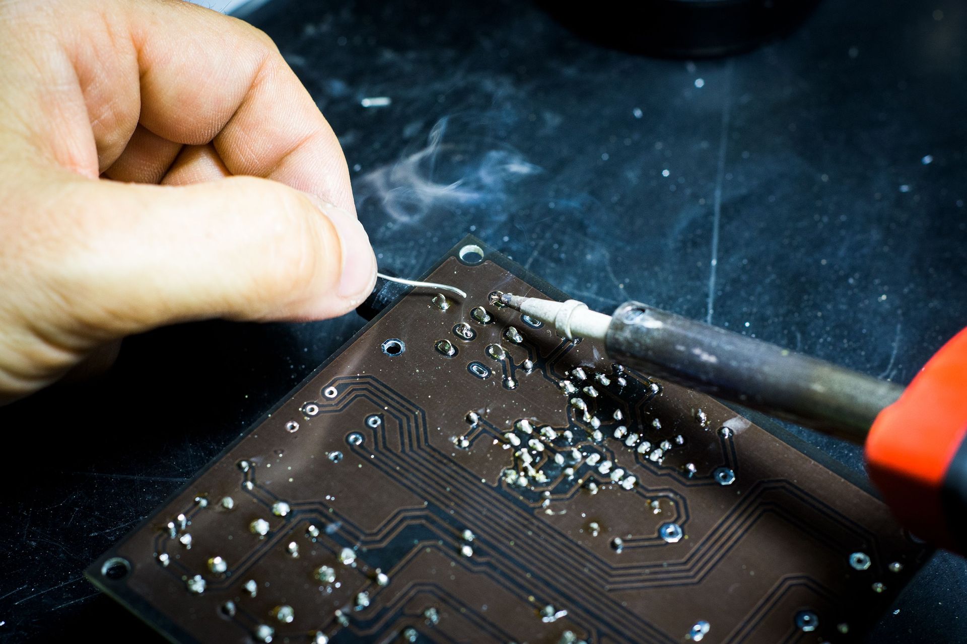
What Is PCB Lamination?
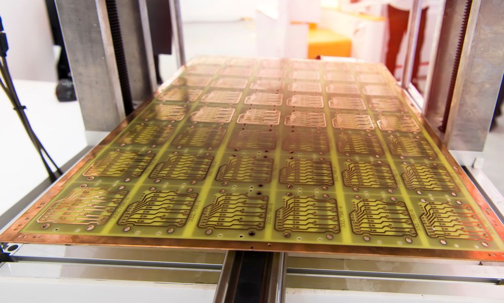
PCB lamination is the controlled process of bonding conductive and insulating layers into a unified multilayer circuit board. Heat and pressure activate the resin within prepreg, which bonds copper-clad cores and other layers according to the specified stackup. It is one stage in how PCBs are made, and its accuracy influences the board’s structural integrity and dimensional stability.
Cores create rigid foundations for copper circuitry, while prepreg fills spaces between adjacent layers and cures into a solid dielectric. Copper layers form the board’s internal conductive paths. Proper bonding and alignment establish the stable construction needed for subsequent drilling, plating, and assembly processes.
How Does the PCB Lamination Process Work?
Lamination follows a controlled sequence based on the approved stackup and material specifications. Early PCB engineering decisions influence layer arrangement, dielectric thickness, copper distribution, and processing parameters.
- Prepare the layers. Fabricated inner layers are cleaned and treated to promote reliable bonding.
- Build the stackup. Cores, copper, and prepreg are positioned in the specified sequence and aligned.
- Apply heat and pressure. A lamination press heats the stack under controlled pressure, causing prepreg resin to flow between adjacent layers.
- Cure and cool. The resin hardens into a stable structure before the panel moves to drilling and other fabrication processes.
Precise process control helps limit voids, misregistration, and inconsistent bonding.
What Materials Are Used in PCB Lamination?
Material selection affects electrical behavior, thermal performance, dimensional stability, and fabrication characteristics. A PCB stackup typically combines several material types selected for the application and operating environment.
| Material | Role in the PCB |
|---|---|
| Core | Provides a rigid, cured dielectric base with copper bonded to one or both sides. |
| Prepreg | Uses partially cured resin and reinforcement to bond adjacent layers during pressing. |
| Copper foil | Forms conductive circuitry on internal and external layers. |
| Specialty laminates | Address specific thermal, electrical, or high-frequency performance needs. |
Factors such as glass transition temperature, coefficient of thermal expansion, dielectric properties, and
PCB laminate availability can influence material decisions before fabrication begins.
Standard vs. Sequential PCB Lamination
The appropriate lamination method depends largely on board architecture, layer count, and interconnect strategy. Standard lamination bonds the primary multilayer stack during one main cycle and suits many conventional through-hole constructions. With fewer processing and thermal cycles, the fabrication sequence is generally less complex.
Sequential lamination builds sections of the PCB through multiple lamination cycles. This approach accommodates certain blind, buried, and microvia structures commonly associated with complex HDI designs. Each additional cycle introduces further registration, processing, and thermal considerations. Reviewing the stackup and via structure early helps engineering teams determine an appropriate construction while balancing routing density, manufacturability, reliability, and production requirements.
Common PCB Lamination Defects and Reliability Risks
Lamination defects can remain hidden inside a multilayer board and emerge after reflow, thermal cycling, or extended service. Identifying these risks before assembly reduces the chance of intermittent electrical problems and later field failures.
- Delamination: Separation between layers can compromise structural integrity and electrical connections.
- Voids: Trapped air or incomplete resin flow can leave weak areas within the dielectric structure.
- Resin starvation: Insufficient resin between layers can reduce bond strength and insulation performance.
- Layer misregistration: Poor alignment can affect drilled-hole accuracy and connections to internal features.
- Microvia interface defects: Weak internal connections may survive initial inspection but fail after repeated thermal stress.
Reliable fabrication depends on controlling materials, processing conditions, and stackup geometry.
How PCB Lamination Affects PCB Assembly and Performance
Lamination quality becomes especially important when a bare board enters PCB production. Reflow exposes the assembly to elevated temperatures that can reveal weak internal bonds, microvia interfaces, or trapped moisture. Dimensional instability and warpage can also affect component placement, solder joint formation, and alignment during automated processes.
Some internal defects may pass initial bare-board inspection yet appear after reflow or repeated thermal cycling. This makes fabrication documentation, material control, and appropriate inspection important inputs to assembly planning. For complex boards, X-ray inspection, electrical testing, and functional testing can add visibility into downstream performance. Strong coordination between fabrication and assembly teams helps reduce unexpected yield problems, rework, and field reliability concerns.
PCB Lamination Considerations for High-Reliability Applications
Medical, aerospace, defense, and industrial electronics may encounter thermal cycling, vibration, extended service life, and challenging operating conditions. Material properties such as Tg, coefficient of thermal expansion, moisture behavior, and dielectric characteristics should align with the intended application.
Stackup design also warrants close review. Dielectric thicknesses, copper distribution, and via structures need to align with fabrication capabilities. Manufacturing teams should account for reflow cycles, potential rework, and operating temperatures when evaluating thermal exposure. Clear material and process traceability adds another layer of control for high-reliability programs. An early DFM review can identify fabrication and assembly concerns while there is still time to address them before production.
How EI Microcircuits Supports Reliable PCB Assembly After Lamination
Once laminated boards reach assembly, process control and verification become central to consistent results. EI Microcircuits applies DFM review, controlled assembly processes, AOI, X-ray inspection, flying probe, in-circuit testing, and functional testing based on product needs. These capabilities help identify assembly concerns and verify performance before products advance into box-build assemblies and final integration.
For high-reliability programs, we focus on traceability, flexibility, and coordinated lifecycle manufacturing. This approach gives OEM teams a single manufacturing partner for PCB assembly, testing, conformal coating, final assembly, and related services while maintaining defined quality processes.
Contact EI Microcircuits today to find a solution to your electronics manufacturing challenges.

let's talk
EI Microcircuits is comprised of three production facilities totaling over 100,000 square feet of climate-controlled manufacturing, engineering and warehousing. We are ready to be the solution to your next project. Contact Us, Request a Quote or Schedule a Tour today!
Manufacturing plant 1
1651 Pohl Road
Mankato, MN 56001
P: 507.345.5786
Manufacturing plant 2
2011 Klein Street
St. Peter, MN 56082
P: 507.934.5722
manufacturing plant 3
69 Power Drive
Mankato, MN 56001
P: 507.386.9160
*Each facility is configured to support your production needs. While maintaining continuity with each other in equipment, training and process control, each facility offers its own specialty. All facilities share the same data center to allow for seamless manufacturing between locations.