What is a PCB? Everything You Need to Know
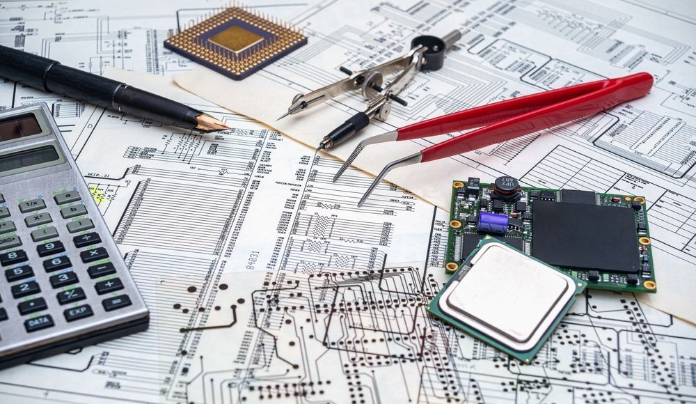
Printed Circuit Boards (PCBs) form the structural and electrical foundation of nearly every electronic device, from basic consumer products to life-saving medical instruments and mission-critical aerospace systems. They support and connect electronic components through carefully designed conductive pathways, enabling complex functions in compact, durable formats.
PCB designs vary widely in layer count, materials, and construction methods depending on the performance demands of the end product. Their quality directly influences reliability, efficiency, and longevity, especially in high-stakes applications. For OEMs developing products that must meet strict regulatory, environmental, or functional standards, understanding the role of the PCB is the first step toward consistent, production-ready outcomes. At EI Microcircuits, that’s where quality begins.
What is a Printed Circuit Board (PCB)?
A Printed Circuit Board (PCB) is a layered structure used to mechanically support and electrically connect electronic components. It consists of conductive copper traces laminated onto a non-conductive substrate, typically FR-4, a glass-reinforced epoxy laminate. These traces form the electrical pathways that route signals and power between components such as resistors, capacitors, microprocessors, and connectors.
PCBs are engineered to precise specifications, accounting for signal integrity, thermal performance, mechanical constraints, and manufacturability. Designs may include single or multiple copper layers, through-hole or surface mount components, and features like blind or buried vias to optimize space and function. Solder masks and silkscreen layers aid in assembly and identification, while coatings or encapsulants provide environmental protection.
A PCB actively shapes system performance. Its design and construction influence everything from signal fidelity to thermal dissipation and mechanical durability. In high-reliability applications, these factors are tightly controlled to prevent failure and maintain consistent function over the product’s full lifecycle.
Board Class
Printed Circuit Boards are categorized into three IPC-defined classes based on their performance and inspection requirements. Each classification reflects different priorities in terms of durability, reliability, and cost, helping manufacturers and OEMs align board construction to end-use expectations.
Class 1
Class 1 boards are designed for general-purpose applications where functionality is the primary concern. These boards are commonly used in consumer electronics and low-risk environments. Visual imperfections are acceptable, and inspections focus on basic operational standards rather than long-term reliability.
Class 2
Class 2 represents the most common classification in industrial and commercial electronics. Boards in this class must exhibit consistent performance over an extended service life. While cosmetic defects are tolerated within limits, electrical reliability and manufacturing consistency are more tightly controlled than in Class 1.
Class 3
Class 3 boards are built for high-performance, high-reliability applications such as aerospace, medical, and military systems. They require rigorous process control and meet the most stringent inspection criteria. Every feature is evaluated for durability, precision, and operational longevity under harsh conditions.
Types of PCBs
The structure of a PCB determines how components are connected and how the circuit performs under physical, thermal, and electrical stresses. From simple layouts to complex, multi-functional systems, each type of PCB serves a distinct purpose based on design needs and end-use conditions.
Single-Sided
Single-sided PCBs have one conductive layer and are typically used in low-density designs. Components are mounted on one side, while copper traces route signals on the other. This configuration offers a straightforward, cost-effective solution for basic electronics with minimal routing complexity.
Double-Sided
Double-sided PCBs feature copper layers on both sides of the substrate. Components can be mounted on either side, allowing for more complex routing and denser designs. Plated through-holes connect the layers, supporting broader functionality than single-sided boards.
Multi-Layer
Multi-layer PCBs stack multiple conductive layers within a single board. These are used when signal routing, grounding, or power distribution must be tightly managed. They offer enhanced electrical performance in compact formats, often found in telecommunications, medical imaging, and defense electronics.
Rigid-Flex
Rigid-flex PCBs combine rigid board sections and flexible interconnects. This hybrid structure reduces the need for connectors and wiring harnesses in compact assemblies. It also adds mechanical durability in applications exposed to motion or vibration.
Flex
Flexible PCBs use thin polyimide or polyester substrates that bend and fold without damaging traces. They’re used in devices requiring space-saving, lightweight circuitry, such as medical wearables, cameras, and aerospace instruments.
Metal Core
Metal core PCBs incorporate a thermally conductive base layer (usually aluminum or copper) to improve heat dissipation. They’re commonly used in LED systems, power converters, and industrial controls where thermal management is a design priority.
Industry Applications of Printed Circuit Boards
Printed Circuit Boards support a wide range of industries, each requiring specific performance characteristics based on electrical, mechanical, and environmental conditions. The versatility of PCB design allows for tailored configurations that match the reliability and functionality expected in each sector.
Aviation & Aerospace
In aerospace systems, PCBs must operate reliably across extreme altitudes, temperature fluctuations, and vibration exposure. Rigid-flex and high-temperature materials are commonly used in flight controls, navigation equipment, and communication modules where performance under stress is non-negotiable.
Agriculture & Farming
Modern farming equipment integrates electronics for GPS tracking, automated planting, soil monitoring, and moisture control. These applications rely on durable PCBs that resist dust, vibration, and temperature swings in outdoor environments.
Automotive
From engine controls to ADAS systems, PCBs are embedded throughout today’s vehicles. Designs must withstand heat, vibration, and electrical interference while maintaining consistent function across long product life cycles. Automotive-grade testing and traceability are key factors.
Consumer Electronics
In high-volume consumer products like smartphones, tablets, and wearables, PCBs must balance performance and miniaturization. Multi-layer and flex boards are used to meet size constraints without sacrificing speed or power efficiency.
Energy & Utility
Power management, grid controls, and renewable energy systems use PCBs to monitor and regulate high-voltage operations. Thermal performance and long-term durability are often prioritized in these designs to prevent failure in mission-critical systems.
Medical
Medical PCBs are used in diagnostic imaging, surgical tools, monitoring equipment, and implantables. These assemblies must meet strict safety and cleanliness standards, often involving specialized coatings, traceability, and tight tolerance control.
Military
Defense electronics rely on Class 3 PCBs for mission assurance in harsh or combat environments. Applications include targeting systems, encrypted communications, and surveillance platforms where failure is not an option.
Telecommunications
Networking infrastructure, satellites, and mobile base stations depend on PCBs that maintain high-frequency signal integrity. Materials must support controlled impedance and thermal stability to sustain bandwidth and uptime in data-intensive systems.
How Are PCBs Manufactured?
PCB manufacturing involves a controlled sequence of processes, each tailored to meet specific design, material, and performance requirements. It begins with imaging the circuit design onto copper-clad laminate, followed by etching to remove unneeded copper and form conductive traces. Layers are then aligned and laminated under heat and pressure for multi-layer boards.
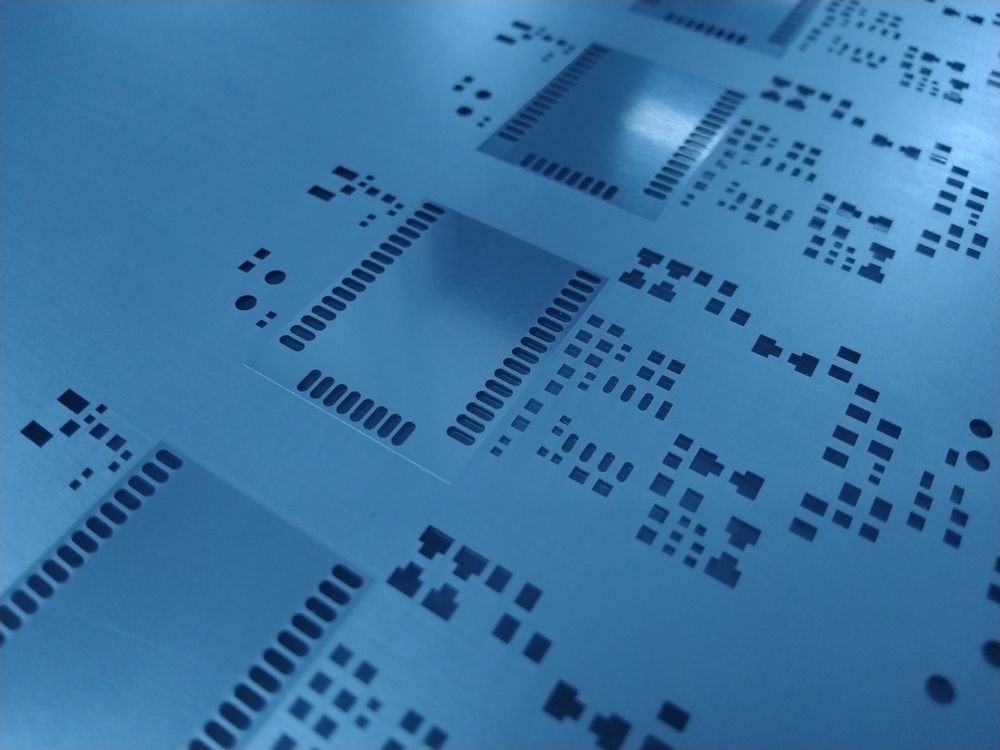
Drilling creates holes for component leads or vias, which are plated to allow electrical connectivity between layers. Surface finishes such as ENIG or HASL are applied to protect exposed copper and improve solderability. At this stage, solder mask and silkscreen are added for protection and identification. Components are placed through surface mount or through-hole processes, then soldered using reflow or wave solder techniques.
Inspection and testing are built into every stage. At EI Microcircuits, we use automated optical inspection (AOI), X-ray imaging, in-circuit testing, and functional test protocols to confirm accuracy and performance before final integration.
From bare board fabrication to complete box-builds, precision and repeatability drive every decision.
Ready to simplify your supply chain and build smarter from the start?
Contact us today to find a solution to your electronics manufacturing challenges.
let's talk
EI Microcircuits is comprised of three production facilities totaling over 100,000 square feet of climate-controlled manufacturing, engineering and warehousing. We are ready to be the solution to your next project. Contact Us, Request a Quote or Schedule a Tour today!
Manufacturing plant 1
1651 Pohl Road
Mankato, MN 56001
P: 507.345.5786
Manufacturing plant 2
2011 Klein Street
St. Peter, MN 56082
P: 507.934.5722
manufacturing plant 3
69 Power Drive
Mankato, MN 56001
P: 507.386.9160
*Each facility is configured to support your production needs. While maintaining continuity with each other in equipment, training and process control, each facility offers its own specialty. All facilities share the same data center to allow for seamless manufacturing between locations.


