Flying Probe Testing: What It Is & How It Works
Even in tightly controlled manufacturing environments, verifying solder joints, trace integrity, and component placement on low-volume assemblies remains a persistent challenge. Traditional test fixtures can introduce delays and high tooling costs that don’t align with fast-turn or high-mix production needs. Flying probe testing offers a flexible alternative. It adapts quickly, operates without custom fixtures, and enables deeper electrical validation early in the build process.
What Is Flying Probe Testing?
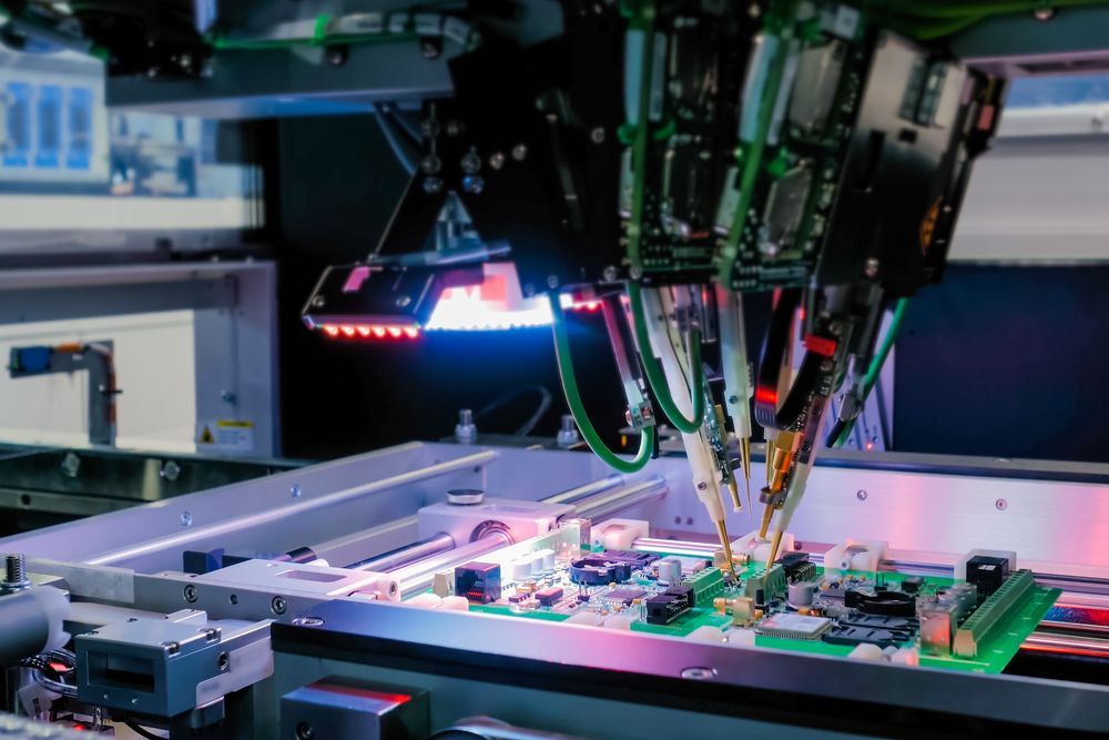
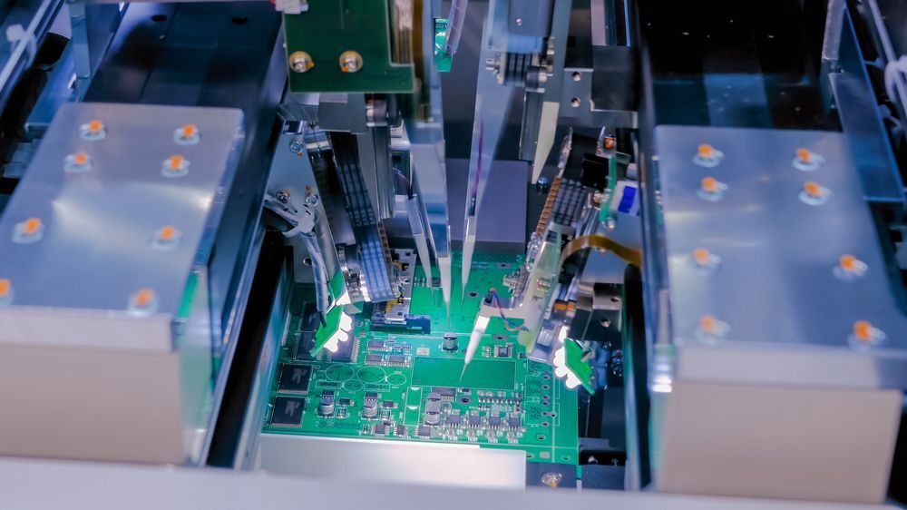
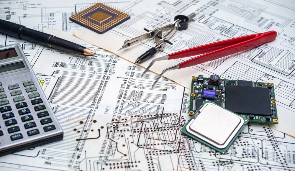
Flying probe testing is a fixtureless electrical test method used to validate printed circuit board assemblies (PCBAs), especially during prototyping or low-volume runs. Instead of relying on a bed-of-nails fixture, it uses a set of movable probes that make contact with test points, vias, and component leads based on programmed coordinates.
This approach facilitates rapid test development and revision without the lead time or cost associated with custom tooling. It’s particularly effective for high-mix environments where assemblies change frequently, or volumes don’t justify permanent fixtures.
At EI Microcircuits, we use this testing as part of a broader quality strategy that includes AOI, X-ray, ICT, and Functional Testing (FCT) to meet the demands of high-reliability markets such as medical, aerospace, and defense.
The Flying Probe Test Process
Testing begins with data-driven programming and ends in real-time electrical validation. The process is flexible, adaptive, and ideal for early-stage or frequently changing assemblies.
Before testing begins, engineers import CAD data or Gerber files to map out the board’s layout and identify accessible test points. This digital model serves as the basis for probe path planning, pin-to-net associations, and component orientation.
Test coverage depends on the quality of the data and the availability of test pads or exposed copper. At EI Microcircuits, we refine this programming phase to align with both design intent and manufacturability constraints. Our team evaluates each net for accessibility, minimizing probe travel time, and optimizing contact accuracy.
Because the system is software-driven, updates to the program can be made quickly. This is especially helpful for teams iterating through multiple board revisions or engineering changes.
Flying probe systems support a variety of electrical tests, including continuity, shorts, resistance, capacitance, and diode polarity. These checks help detect common assembly issues such as missing components, incorrect orientation, solder bridges, and opens. Advanced systems also perform powered tests like boundary scan or limited functional verification.
At EI Microcircuits, we integrate these test types based on product requirements, IPC standards, and customer-specific test protocols. The non-invasive nature of the probe tips means sensitive components remain protected while still undergoing precise evaluation.
Combined with other inspection methods, this testing contributes to a layered quality assurance process that reinforces traceability and defect reduction. This is especially important in assemblies where full in-circuit test coverage may not be practical.
Benefits of Flying Probe Testing
This method offers distinct advantages for OEMs managing high-reliability, low-to-medium volume production. Its flexibility reduces the burden of fixture design and accelerates time-to-test for new products or revisions. At EI Microcircuits, we use this approach to strengthen quality across diverse product lines.
Key benefits include:
- No custom fixture required — reduces setup costs and speeds up test deployment
- Rapid program changes — supports engineering revisions without delay
- High fault coverage — detects opens, shorts, orientation errors, and more
- Non-destructive probing — protects sensitive or densely packed components
- Low NRE investment — suitable for prototypes, pilot runs, and ongoing changes
- Scalable across product types — ideal for varied designs in a high-mix environment
Limitations and Considerations
While this method is versatile, it is not ideal for every production environment. The mechanical nature of the probes and the sequential test process can introduce time constraints, particularly for high-volume builds. Understanding its constraints helps in choosing the right mix of test strategies.
Key considerations include:
- Slower cycle times compared to in-circuit or functional testers for large batches
- Limited access to assemblies without dedicated test pads or exposed copper
- Mechanical wear on probe tips necessitates periodic maintenance
- Board-level focus only, not intended for complete system-level validation
- Test coverage depends on available CAD data and board layout
- Less practical for high-speed, high-throughput test environments
Ideal Use Cases
This test is well-suited for applications where flexibility, traceability, and speed of deployment matter more than test throughput. It fills a critical role in early-stage builds, high-mix production, and situations where custom test fixtures are impractical or cost-prohibitive.
Common use cases include:
- Prototyping and NPI, where frequent design revisions require adaptable test coverage
- Low- to medium-volume production where fixture investment isn’t justified
- High-complexity assemblies that benefit from precise validation without overhandling
- High-reliability sectors such as medical, aerospace, or defense, where fault isolation is key
- DFM feedback loops during pilot runs, enabling quick corrections based on test results
- Mixed-technology boards, where physical access limits fixture-based methods
EI Microcircuits’ Advanced Test Capabilities
EI Microcircuits applies a systems-based approach to testing that aligns with our quality management systems and the requirements of high-reliability sectors. Our flying probe testing is integrated into a broader test strategy that includes AOI, X-ray, in-circuit testing, and full functional validation. We manage a range of broad types, from simple single-sided boards to dense, multilayer designs with limited access.
Our testing protocols are built around
IPC class certifications, customer specifications, and end-use reliability expectations. We maintain
certifications such as ISO 13485 and AS9100D, which guide our processes in regulated industries.
This closed-loop approach helps reduce defect rates, strengthens traceability, and sustains long-term product performance through the manufacturing lifecycle.
Supporting Services for Test-Driven Manufacturing
This method is most effective when paired with a comprehensive test and inspection strategy. At EI Microcircuits, we combine PCB inspection methods such as Automated Optical Inspection (AOI), X-ray analysis, and in-circuit testing to catch issues at multiple stages. This layered approach reduces risk and reinforces validation from the first article through final shipment.
No matter your desired path for end-of-the-line test services, our Test Engineering group can develop a solution to meet your requirements. Our team can design, develop, and implement a test strategy and system to meet the needs of your specific project.
We also handle conformal coating, overmolding, and box-build integration to support customers seeking full product realization under one roof. Our teams collaborate early in the design phase to streamline test access, enhance manufacturability, and limit rework.
To learn how our test capabilities can support your quality goals,
contact us today to start a conversation about your next high-reliability build.
let's talk
EI Microcircuits is comprised of three production facilities totaling over 100,000 square feet of climate-controlled manufacturing, engineering and warehousing. We are ready to be the solution to your next project. Contact Us, Request a Quote or Schedule a Tour today!
Manufacturing plant 1
1651 Pohl Road
Mankato, MN 56001
P: 507.345.5786
Manufacturing plant 2
2011 Klein Street
St. Peter, MN 56082
P: 507.934.5722
manufacturing plant 3
69 Power Drive
Mankato, MN 56001
P: 507.386.9160
*Each facility is configured to support your production needs. While maintaining continuity with each other in equipment, training and process control, each facility offers its own specialty. All facilities share the same data center to allow for seamless manufacturing between locations.