Everything to Know About Solder Masks in PCBs
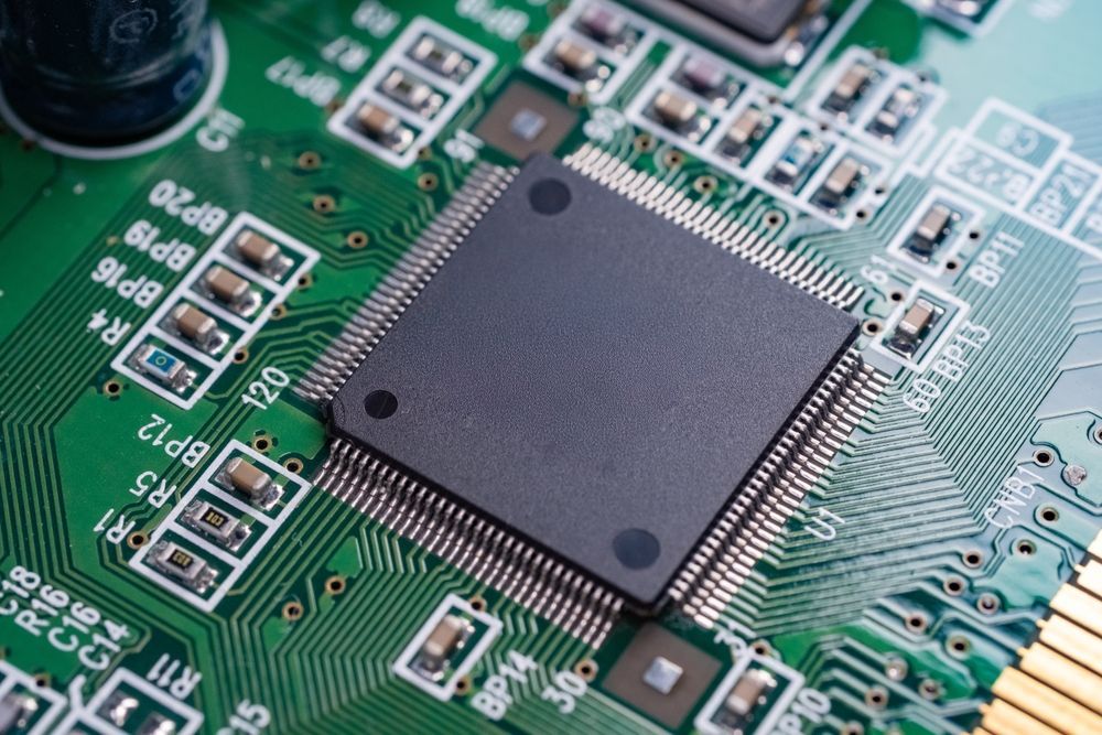
Printed circuit boards often appear simple on the surface. Copper layers, pads, and traces work together to deliver function. But reliable performance depends on more than conductive paths. The solder mask layer plays a quiet but important role in protecting connections, guiding assembly, and enhancing product consistency.
What is a Solder Mask Layer?
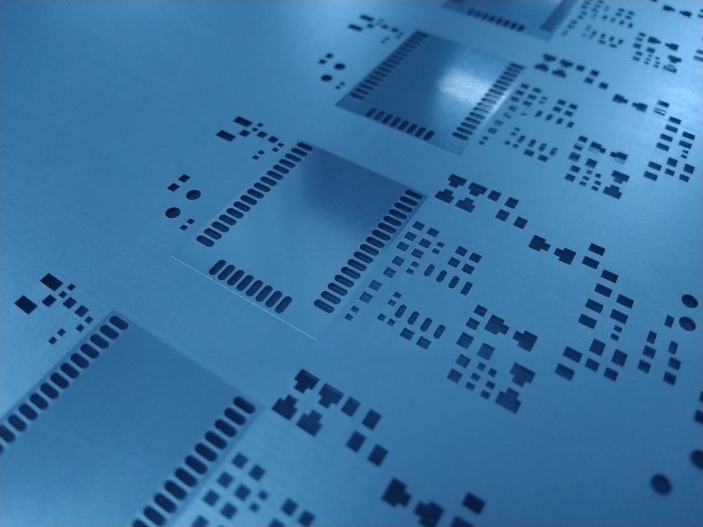
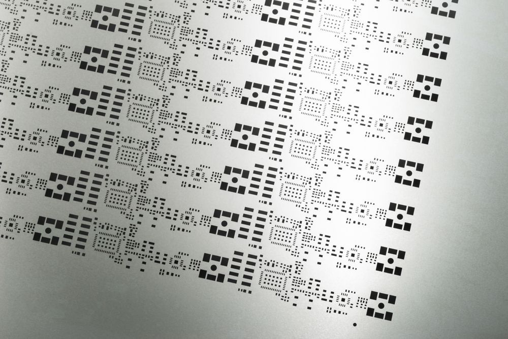
A solder mask is a protective polymer layer applied over the copper traces of a printed circuit board. It isolates conductive areas from environmental exposure and helps prevent solder bridging during assembly. The layer defines where solder should and should not adhere, enabling precise component placement and cleaner joints. Most designs rely on it to stabilize reflow processes and extend long-term reliability.
Primary Functions of a Solder Mask
Solder masks serve both protective and functional roles in
PCB design. They prevent oxidation and contamination of copper features, block unintended solder flow during assembly, and reduce the risk of shorts between fine-pitch components. The layer also supports automated optical inspection by providing contrast against exposed metal. In high-reliability assemblies, solder masks contribute to mechanical stability and long-term electrical isolation.
Types of Solder Mask Materials
Different PCB applications call for different solder mask materials. Each type brings unique characteristics based on processing method, resolution, and durability.
Epoxy
Epoxy-based solder masks are the most economical option, applied using silkscreen printing. Once cured, they offer basic protection against moisture and oxidation. While acceptable for low-complexity designs, epoxy lacks the fine resolution and chemical resistance needed for high-density or harsh-environment applications in cost-sensitive legacy manufacturing contexts.
LPI
Liquid Photoimageable (LPI) solder masks are the standard in modern PCB fabrication. Applied through spraying or curtain coating, they are then UV-exposed and developed for precise patterning. It’s widely used in
sectors we partner with, particularly those demanding traceability, durability, and process repeatability in regulated or high-reliability environments.
Dry Film
Dry film solder masks are laminated onto the PCB surface and then patterned through exposure and development. They yield excellent edge definition and are used when extremely tight registration is required. Though more labor-intensive and costly than LPI, dry film masks remain common in builds needing superior dimensional control or specialty finishes.
Solder Mask Application Methods
The method used to apply a solder mask affects alignment accuracy, surface coverage, and yield. Techniques include screen printing for epoxy masks, curtain coating for LPI, and lamination for dry film. After application, the material is exposed to UV light through a photomask to define openings. Post-development curing hardens the layer, locking in its protective and functional properties for final assembly.
DFM Guidelines for Solder Mask Design
Designing solder mask features for manufacturability reduces rework and boosts yield. Follow these principles:
- Maintain adequate mask clearance around pads and vias.
- Avoid mask slivers between fine-pitch leads.
- Keep the minimum solder mask dam width above fabrication limits.
- Align solder mask openings accurately to pad geometry.
These practices reduce bridging, strengthen inspection reliability, and help avoid delamination during thermal cycling.
Popular Solder Mask Colors
Solder mask color affects not just appearance but also function. Different hues vary in contrast, heat resistance, and light reflectivity, which can influence inspection, rework, and product identity.
Green
Green is the most commonly used solder mask color due to its balance of performance and visibility. It offers high contrast for both manual inspection and automated optical systems. Its thermal stability and chemical resistance support use in demanding applications, including medical and aerospace assemblies.
Red
Red solder masks are chosen for aesthetic differentiation or internal identification. While they show moderate contrast and durability similar to green, they may reflect more light under inspection. They are generally used in consumer and industrial builds where visual uniqueness is preferred.
Blue
Blue masks present a matte finish and slightly softer contrast, which can help visual inspection in specific lighting. They are used in test boards or branded products. Though their performance matches other colors, the surface may highlight flux or residue, prompting careful handling.
Black
Black solder masks absorb both heat and light, affecting thermal behavior during reflow. The dark finish reduces contrast, making visual or optical inspection more difficult. However, they are selected when a low-reflective or enclosed design requires a darker appearance.
White
White solder masks reflect heat and light, which presents challenges during reflow but benefits LED-based or optical assemblies. Their brightness can reveal contamination, so extra attention may be needed during cleaning. They are often used when lighting behavior must be managed within the design.
Yellow
Yellow offers limited contrast, which complicates both manual and automated inspection. It is rarely seen in high-reliability production and is mostly used for specialty prototypes or niche visual requirements. Limited functional benefit keeps it from widespread adoption.
Common Issues and Defects in Solder Mask Application
Solder mask defects can compromise board reliability. Issues include misalignment, pinholes, underdeveloped openings, and delamination. Contamination during processing can reduce adhesion or form voids. In high-density layouts, mask slivers between pads may lift or crack during reflow. Careful inspection using AOI, X-ray, or flying probe testing detects these faults before final assembly.
Solder Mask vs. Other Protective Coatings
Solder masks shield traces during assembly. Conformal coatings protect the full assembly later, often against moisture, dust, and chemical exposure. The solder mask defines where solder bonds, while the coating guards finished components. Both are common in high-reliability builds, but they address separate risks across the manufacturing timeline.
Partnering with EI Microcircuits
We work with OEMs that value precision, traceability, and process control. Our approach integrates solder mask accuracy, DFM consultation, and full lifecycle manufacturing under one roof. We apply control across every stage, using layout validation and test coverage to reduce risk and enhance quality. Our background in Electronics Manufacturing Services (EMS) helps customers manage complexity while maintaining consistency.
If your products demand consistent performance and expert oversight,
reach out to discuss how we align technical needs with production outcomes.
Key Takeaways
Solder masks define solderable areas, assist inspection systems, and protect conductive paths throughout the PCB lifecycle. Material choice, application method, and layout design directly affect performance. For OEMs managing the
costs of PCBs and PCBA, solder mask precision reduces scrap, limits failures, and strengthens field reliability. When reliability and partnership are priorities, EI Microcircuits builds to that standard.


let's talk
EI Microcircuits is comprised of three production facilities totaling over 100,000 square feet of climate-controlled manufacturing, engineering and warehousing. We are ready to be the solution to your next project. Contact Us, Request a Quote or Schedule a Tour today!
Manufacturing plant 1
1651 Pohl Road
Mankato, MN 56001
P: 507.345.5786
Manufacturing plant 2
2011 Klein Street
St. Peter, MN 56082
P: 507.934.5722
manufacturing plant 3
69 Power Drive
Mankato, MN 56001
P: 507.386.9160
*Each facility is configured to support your production needs. While maintaining continuity with each other in equipment, training and process control, each facility offers its own specialty. All facilities share the same data center to allow for seamless manufacturing between locations.