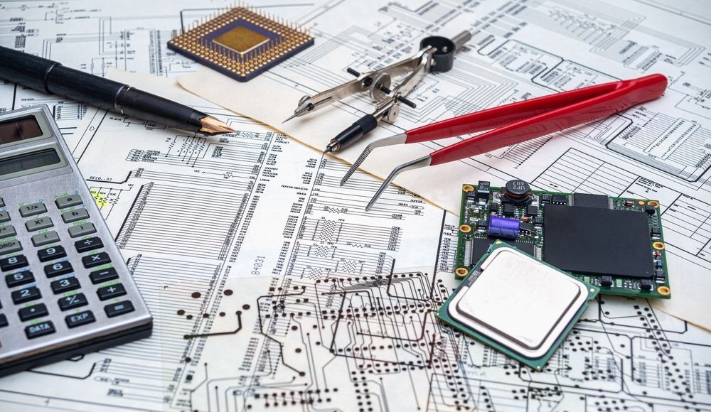
Through-Hole vs Surface Mount: Key Differences Explained
Every circuit begins with a decision about how its components will meet the board. It’s a small detail with large consequences. One that shapes not only performance, but reliability, serviceability, and even how the final product feels in use.
Some designs demand the dense precision of surface mount technology, where components rest neatly on the surface. Others depend on the enduring strength of through-hole leads that anchor parts deep into the substrate. Each method carries its own logic, evolved from decades of engineering tradeoffs between size, speed, and durability. Understanding those distinctions helps designers and manufacturers work with intention, not habit.
Understanding the Two Technologies
What is Surface Mount Technology (SMT)
Surface Mount Technology places components directly onto the surface of a printed circuit board. Pads replace drilled holes, allowing for smaller parts, tighter spacing, and automated placement. The result is higher circuit density and faster production, ideal for compact, high-performance devices. SMT supports double-sided assembly and enables miniaturization across medical, aerospace, and industrial products where precision and efficiency matter most.
What is Through-Hole Technology
Through-hole assembly mounts components by inserting their leads through drilled holes and soldering them to pads on the opposite side. This creates a stronger mechanical bond, critical for connectors, transformers, and high-stress environments. While it requires more space and labor, through-hole technology remains essential where durability and long-term reliability outweigh size constraints.
Key Differences Between Through-Hole and Surface Mount
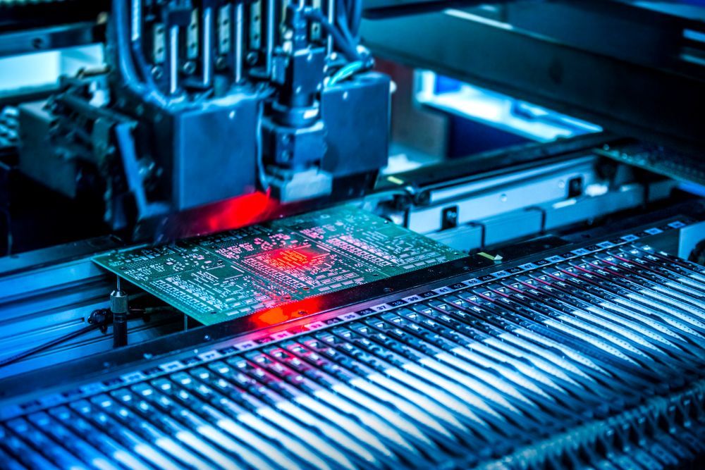
Assembly Process
Surface Mount (SMT):
- Components placed by automated pick-and-place machines.
- Soldered using a reflow oven for high precision and speed.
- Ideal for high-volume production and repeatability.
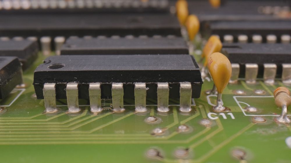
Through-Hole (THT):
- Leads inserted into drilled holes and soldered by wave soldering or hand.
- More manual labor and longer cycle times.
- Favored for prototypes, connectors, and heavy components.
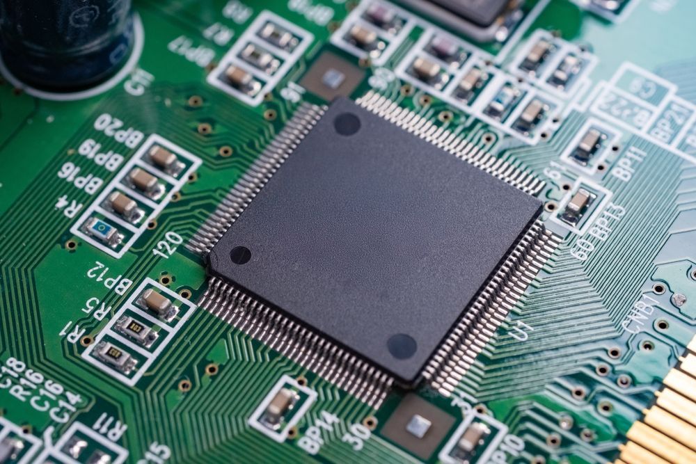
Component Size and Density
Surface Mount (SMT):
- Extremely small components (e.g., 0201, 0402 packages).
- Mountable on both sides of the PCB.
- Enables high circuit density and compact design.
Through-Hole (THT):
- Larger components requiring drilled vias.
- Single-sided mounting limits density.
- Best suited for assemblies where size is less critical.
Mechanical Strength
Surface Mount (SMT):
- Components soldered only to surface pads.
- Sufficient for stable, low-vibration environments.
- More fragile under mechanical stress or torque.
Through-Hole (THT):
- Leads pass through the board for stronger mechanical anchoring.
- Withstands vibration, thermal cycling, and repeated insertion forces.
- Common in aerospace, defense, and industrial applications.
Electrical Performance
Surface Mount (SMT):
- Shorter electrical paths improve high-frequency performance.
- Reduced parasitic effects benefit fast signal transmission.
- Ideal for RF, digital, and high-speed circuitry.
Through-Hole (THT):
- Longer signal paths increase inductance and capacitance slightly.
- Supports higher current loads and power components reliably.
- Preferred for high-voltage or high-thermal-stress environments.
Inspection and Testing
Surface Mount (SMT):
- Relies on Automated Optical Inspection (AOI), X-ray, and ICT.
- Detects fine-pitch defects not visible to the eye.
- Rework can be complex due to component density.
Through-Hole (THT):
- Easier manual inspection of visible solder joints.
- Simplifies rework and functional testing.
- Useful for early-stage validation and mixed-technology builds.
Advantages & Disadvantages
Surface Mount Technology (SMT)
SMT offers exceptional efficiency and precision. Its components are small, lightweight, and compatible with high-speed automated placement, enabling dense circuit layouts and reduced material use. The shorter signal paths support excellent high-frequency performance and low parasitic losses, which are essential in medical instrumentation, aerospace electronics, and advanced communication systems. These benefits translate into smaller, faster, and often more cost-effective assemblies once tooling is in place.
However, the same miniaturization that drives performance can also complicate repair and rework. Components are tightly spaced, solder joints are smaller, and some terminations, such as BGAs, are hidden beneath the package, requiring X-ray inspection. SMT joints also have less mechanical strength, making them less suitable for applications involving repeated stress, direct mechanical load, or extreme vibration.
Through-Hole Technology (THT)
Through-hole assembly excels where mechanical integrity and long-term reliability are critical. Leads that pass through the board create a robust physical bond, allowing the assembly to endure vibration, shock, and thermal cycling. It’s the logical choice for connectors, switches, large capacitors, and power devices. Through-hole also supports easier manual inspection, rework, and prototyping, making it valuable for engineering validation or low-volume, high-reliability builds.
The trade-offs are mainly spatial and procedural. Drilling through the PCB increases manufacturing time and cost, while the larger components limit density and miniaturization. THT’s manual or semi-automated processes are slower and less scalable than SMT, which makes it less practical for high-speed, high-volume production. Still, in environments where performance depends on durability and secure interconnection, through-hole technology remains indispensable.
Ideal Applications for Surface Mount (SMT)
Surface Mount Technology excels in products that demand compactness, precision, and repeatability. Its ability to accommodate extremely small components and high circuit density makes it indispensable for miniaturized, high-performance electronics.
In the medical sector, SMT drives the design of implantable and portable diagnostic devices, where size, weight, and energy efficiency are critical. In aerospace systems, it supports lightweight avionics, data processors, and sensor arrays that require flawless signal integrity under tightly controlled tolerances. Within industrial automation, SMT enables complex control boards and communication modules that must perform reliably in compact enclosures.
SMT excels when reliability depends on precision manufacturing rather than mechanical reinforcement. It enables elegant, tightly integrated designs that prioritize electrical performance, repeatability, and efficient use of board space.
Ideal Applications for Through-Hole
Through-hole assembly is chosen for designs where mechanical strength, serviceability, and thermal endurance take precedence over miniaturization. It’s foundational in environments that expose assemblies to vibration, torque, or elevated temperatures.
In aerospace and defense, through-hole connections anchor power components, switches, and connectors that must survive long mission cycles and extreme vibration. In industrial systems, it supports relays, transformers, and field-replaceable modules that experience physical stress or repeated handling. Even in medical instrumentation, THT remains relevant for high-reliability power supplies and interface hardware that require durable interconnects.
The technology also supports development and repair flexibility. Engineers often use through-hole components in prototypes or mixed-technology builds where access, testing, and manual soldering are necessary. Despite its slower assembly rate, through-hole maintains a vital role wherever endurance, maintainability, and field reliability define product success.
Hybrid PCB Assemblies
Hybrid assemblies integrate both SMT and THT on the same board to balance density, performance, and durability. This approach recognizes that most advanced electronics blend delicate logic with rugged power and interface requirements.
A hybrid layout might pair SMT-mounted microprocessors and ICs for high-speed control with through-hole connectors, inductors, or transformers for mechanical stability and current handling. In medical imaging systems, flight-control electronics, and industrial robotics, this combination allows high-frequency precision and structural reinforcement to coexist.
Hybrid designs represent the most complete expression of modern electronics manufacturing. This leverages automation where possible and mechanical strength where necessary. They reflect a system-level mindset: the right technology, in the right place, for the right function.
Why Partner with EI Microcircuits
Selecting the right assembly method only matters when it’s executed with precision and process control. At EI Microcircuits, we integrate all three under one roof, managed through disciplined quality systems such as ISO 13485 and AS9100D. That structure allows our engineering and production teams to tailor every build to the functional requirements of the product, not just the limitations of the process.
Our manufacturing lines support high-density SMT placement, selective and wave soldering for through-hole components, and seamless hybrid sequencing. Every assembly passes through automated optical inspection, X-ray analysis, and in-circuit or functional testing to confirm performance and reliability.
We operate as an extension of our customers’ manufacturing, by collaborating early in the design cycle to optimize for manufacturability, reduce risk, and support full product lifecycle needs. For OEMs in medical, aerospace, defense, and industrial markets, that means consistent quality, clear communication, and a manufacturing partner prepared to deliver solutions as complex and reliable as the systems they serve.
Contact EI Microcircuits today to explore how our assembly capabilities can support your next high-reliability build. Together, we’ll design and deliver electronics built to perform.
let's talk
EI Microcircuits is comprised of three production facilities totaling over 100,000 square feet of climate-controlled manufacturing, engineering and warehousing. We are ready to be the solution to your next project. Contact Us, Request a Quote or Schedule a Tour today!
Manufacturing plant 1
1651 Pohl Road
Mankato, MN 56001
P: 507.345.5786
Manufacturing plant 2
2011 Klein Street
St. Peter, MN 56082
P: 507.934.5722
manufacturing plant 3
69 Power Drive
Mankato, MN 56001
P: 507.386.9160
*Each facility is configured to support your production needs. While maintaining continuity with each other in equipment, training and process control, each facility offers its own specialty. All facilities share the same data center to allow for seamless manufacturing between locations.