A Guide to Design for Manufacturing in PCBs
Design for manufacturing (DFM) in PCB production improves yield, reduces rework, and shortens time to market. It aligns engineering intent with production realities, bridging what’s theoretically possible and what can be reliably built. Teams that prioritize DFM early catch potential issues before they disrupt schedules, add cost, or compromise performance. For regulated and high-reliability builds, that foresight matters.
Well-implemented DFM practices also differentiate experienced
electronic manufacturing services (EMS) providers who understand how to bridge design intent with scalable production.
What is Design for Manufacturing?
DFM is the practice of engineering PCB layouts to align with real-world production capabilities. It reduces variability, simplifies processes, and minimizes manufacturing risk, particularly in high-mix, high-reliability environments. At its core, DFM enables repeatable outcomes across production runs while improving product quality and cost efficiency. It also shortens validation cycles and helps teams avoid delays caused by late-stage redesigns or test failures.
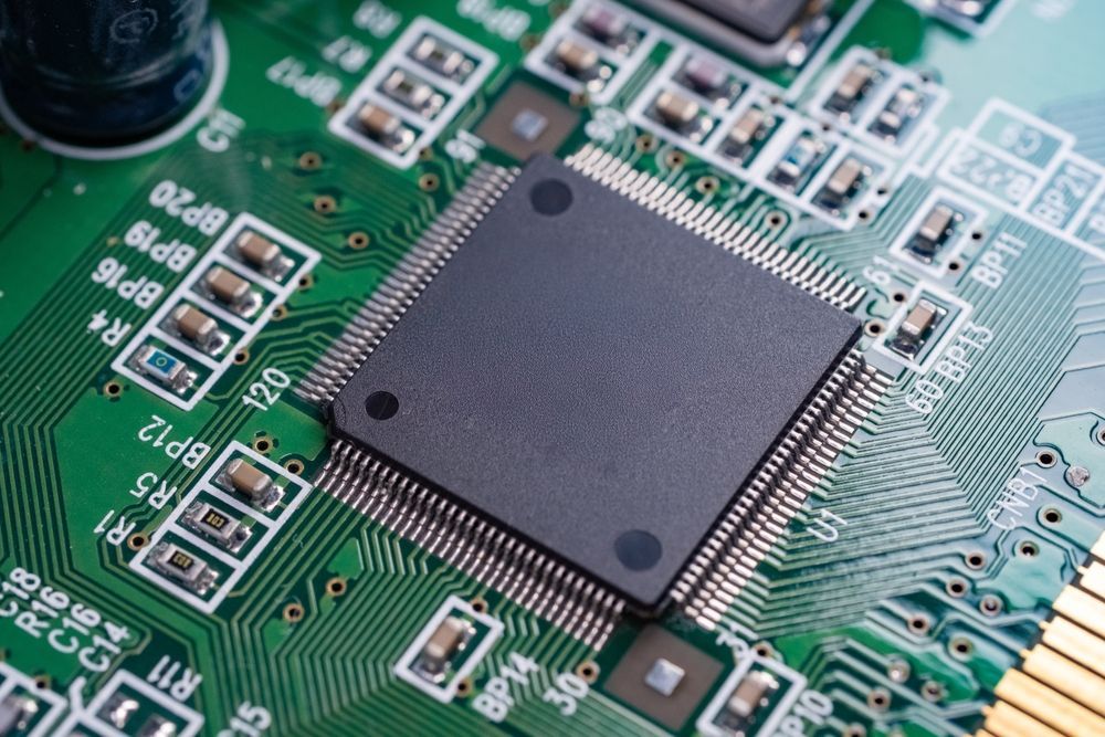
Key aspects of DFM in PCB design include optimizing pad sizes and spacing, matching component layout to automated assembly processes, anticipating thermal and mechanical constraints, preventing soldering and inspection complications, and aligning trace and via design to fabrication limits. These considerations improve throughput, minimize rework, and reduce the need for costly design iterations.
Why is Design for Manufacturing Important?
DFM reduces production delays, scrap, and rework by aligning design intent with manufacturing realities. In industries like medical, aerospace, and defense, even minor deviations can compromise reliability, trigger compliance issues, or delay time-to-market. Incorporating DFM early allows engineering teams to account for material constraints, assembly tolerances, and inspection requirements before designs reach the floor.
It also results in more predictable lead times and better cost control over the product lifecycle. For OEMs managing complex supply chains, DFM provides a structured way to reduce risk while improving manufacturability at scale. It moves quality upstream and gives manufacturers fewer variables to manage during production.

Understanding the DFM Process
DFM is most effective when applied early and revisited throughout product development. It’s a closed-loop process that connects design, engineering, and manufacturing teams to identify constraints and optimize build quality before full production begins.
Typical steps in the DFM process include:
Design Input Review – Evaluate schematics, layout, and BOM against known manufacturing capabilities
Preliminary Feedback – Identify high-risk features or mismatches in tolerances, materials, or assembly methods
Design Optimization – Recommend layout changes to improve solderability, inspection access, and yield
Prototype Validation – Build and test small batches to confirm manufacturability
Production Readiness Sign-off – Final DFM check before full-scale release
Core DFM Principles for PCB Design
Strong DFM practices reduce variation and make PCB designs easier to build, inspect, and test. These principles help maintain quality throughout the product lifecycle and reduce delays during NPI.
Effective layout strategies begin with proper component spacing to allow automated placement, soldering, and rework. Good thermal management includes balanced copper pours and layout symmetry to handle heat dissipation. Panelization must support efficient material use and low-stress depanelization. Designers should incorporate accessible test points for flying probe, ICT, or functional testing. Materials and finishes should meet environmental and regulatory needs, and trace geometry and via structures must comply with fabrication standards.
Common DFM Pitfalls and How to Avoid Them
Even well-designed PCBs can run into manufacturability issues when key production constraints are overlooked. Addressing these pitfalls early in the design process reduces delays, rework, and unexpected costs.
Common pitfalls and solutions:
Tight Component Clustering – Space parts to allow automated placement and soldering without bridging
Unspecified Test Points – Add test features to enable inspection and electrical validation
Mixed Assembly Constraints – Flag areas requiring hand soldering or selective processing during DFM review
Inadequate Pad Design – Follow IPC standards to improve joint integrity and reworkability
Poor Thermal Relief – Avoid heat trapping by optimizing copper connectivity on pads and planes

How EI Micro Supports DFM at Every Stage
We apply DFM across all phases of production, starting at engineering review and continuing through final test and box-build. Our closed-loop NPI workflow brings together layout review, material selection, and manufacturing feedback before the first build. DFM includes pad geometry optimization, thermal profiling, and test point analysis based on IPC and customer-specific requirements.
In-house capabilities like AOI, X-ray, flying probe, and in-circuit testing allow us to validate assumptions quickly and refine designs in real time. This hands-on collaboration reduces turnaround time, avoids miscommunication between design and production, and gives OEM teams a structured way to improve manufacturability across revisions.
Tools and Technologies That Enhance DFM
We use a combination of analysis tools and in-house inspection systems to reduce risk throughout the build process. These technologies help catch issues earlier, reduce manual intervention, and improve process control across every stage of production.
DFM Software Analysis – Identifies spacing, drill, and mask violations early in the layout phase
AOI (Automated Optical Inspection) – Detects solder defects, polarity errors, and missing components after placement
X-ray Inspection – Verifies solder joint quality on hidden leads such as BGAs and QFNs
Flying Probe and ICT – Validates electrical performance and verifies continuity without custom fixtures
3D Solder Paste Inspection (SPI) – Confirms proper paste volume and deposition before reflow
The ROI of DFM-Driven PCB Design
Investing in DFM early yields measurable returns across the product lifecycle. Fewer design iterations, faster prototyping, and lower defect rates all contribute to reduced total cost of ownership. DFM reduces reliance on engineering change orders, which often delay production and increase overhead. It also improves first-pass yield, cutting down rework and scrap during early builds.
In regulated markets, DFM helps teams stay compliant without costly redesigns or requalification. Beyond cost, it improves production stability, simplifies sourcing, and supports
more accurate forecasting. For OEMs managing multiple product lines or revisions, these gains translate directly into greater efficiency and supply chain predictability.
Partnering with EI Micro for DFM Success
We work closely with OEMs to integrate DFM early in development, aligning layout decisions with real-world manufacturing constraints. Our team reviews design packages for process compatibility, identifies risks, and provides feedback that directly improves production outcomes. Every recommendation reflects experience across medical, aerospace, and industrial sectors, covering layout strategy, pad design, thermal behavior, and testability.
This involvement extends beyond the prototype. We handle each build through testing, box-build integration, and full-rate production. Our services include assembly, inspection, coating, and final integration, all managed under one roof to reduce vendor complexity and compress lead times. The result is a stable, proven process and a manufacturing partnership built for long-term success.
Contact EI Microcircuits to review your design package and take the next step toward reliable, production-ready PCB assemblies.

let's talk
EI Microcircuits is comprised of three production facilities totaling over 100,000 square feet of climate-controlled manufacturing, engineering and warehousing. We are ready to be the solution to your next project. Contact Us, Request a Quote or Schedule a Tour today!
Manufacturing plant 1
1651 Pohl Road
Mankato, MN 56001
P: 507.345.5786
Manufacturing plant 2
2011 Klein Street
St. Peter, MN 56082
P: 507.934.5722
manufacturing plant 3
69 Power Drive
Mankato, MN 56001
P: 507.386.9160
*Each facility is configured to support your production needs. While maintaining continuity with each other in equipment, training and process control, each facility offers its own specialty. All facilities share the same data center to allow for seamless manufacturing between locations.