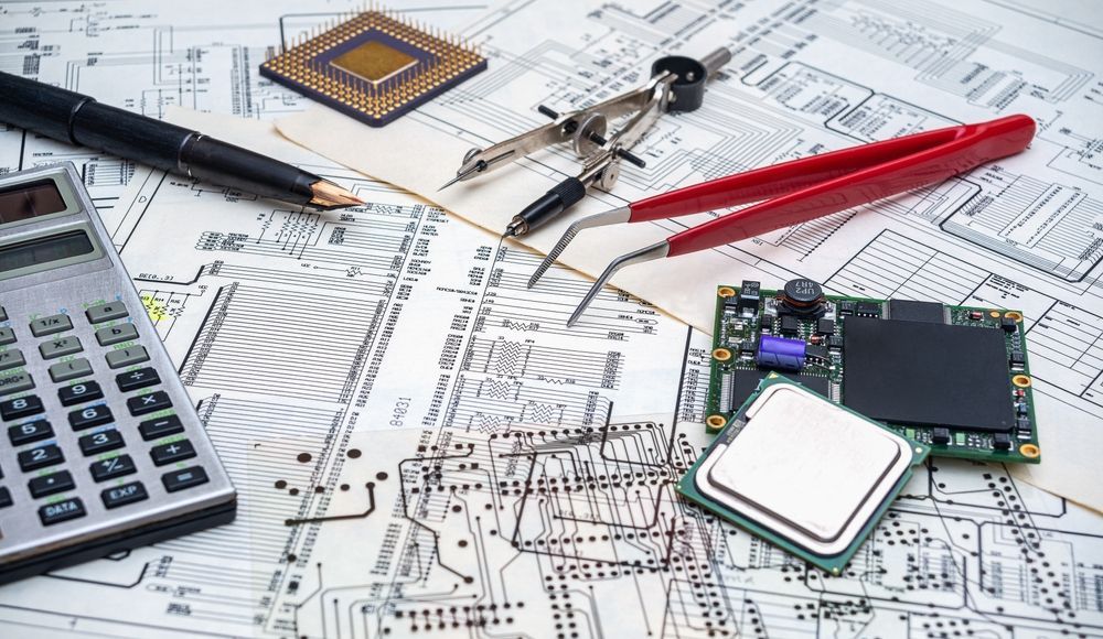
The Ultimate Guide to Electrical Potting
Sensitive electronics often operate in harsh environments. Vibration, moisture, dust, and heat all introduce potential failure points. Many assume that the enclosure provides sufficient protection. In reality, internal components remain exposed. Potting creates a sealed barrier around the electronics, extending reliability and reducing mechanical and environmental stress.
Key Takeaways
Potting electronics protects assemblies from harsh conditions, reinforces mechanical structure, and extends service life. Material selection, process consistency, and proper validation shape performance over time. In high-reliability builds, potting adds durability where traditional enclosures fall short.
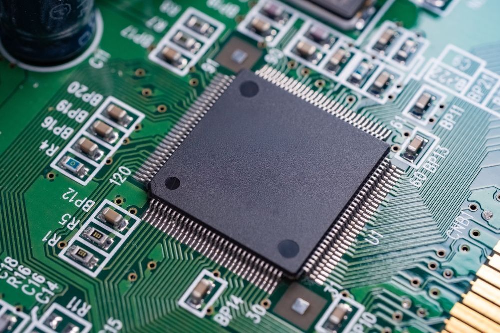
What is Electrical Potting?
Electrical potting involves surrounding an electronic assembly in a liquid compound that hardens into a protective shell. The process isolates sensitive components from moisture, vibration, and corrosive agents.
PCB potting materials fill air gaps and conform to complex geometries, making it effective for both standard and high-reliability applications. It's commonly used in assemblies where long-term stability or harsh environmental exposure is expected.
Core Functions of Potting
Potting strengthens mechanical stability, enhances insulation, and protects against thermal cycling and contamination. It shields components from shock, vibration, and chemical exposure while also reducing the risk of arcing or shorts. In assemblies subject to field use or transport, potting helps maintain performance over time. For mission-critical electronics, it acts as a safeguard against unpredictable conditions during operation.
Common Types of Potting Compounds
Potting materials vary in hardness, flexibility, chemical resistance, and thermal properties. The right choice depends on performance needs, environmental conditions, and production timelines.
Epoxy
Epoxy compounds are known for their high strength, thermal stability, and excellent adhesion to most surfaces. Once cured, they form a rigid shell that resists moisture and mechanical stress. Epoxies are commonly used in power electronics and automotive assemblies. However, they are brittle under thermal expansion and not ideal for components that experience frequent temperature cycling or flexing during use.
Urethane
Urethanes are more flexible than epoxies, making them well-suited for applications that require impact resistance or vibration damping. They cure to a softer finish and block moisture, solvents, and mechanical stress. Urethane potting works well for consumer electronics, industrial controls, and assemblies where components may shift slightly during use. They generally cure at lower temperatures, which supports compatibility with heat-sensitive parts.
Silicone
Silicone potting compounds handle wide temperature ranges and remain flexible after curing. They perform well in assemblies exposed to heat, cold, or UV radiation. Silicones are often used in aerospace, lighting, and outdoor environments where both flexibility and environmental resistance are priorities. While they may have longer cure times, their performance in extreme conditions offsets that limitation for many high-reliability builds.
Selecting the Right Compound for Your Application
Material selection depends on more than chemistry. Engineers must account for curing conditions, bond strength, electrical properties, and service environment. For instance, high-heat exposure may favor silicone, while rigid structural needs may point to epoxy. In mixed-technology builds or variable climates, urethanes often strike the right balance. Matching material characteristics to the mechanical and thermal stress profile increases stability and reduces failure risk.
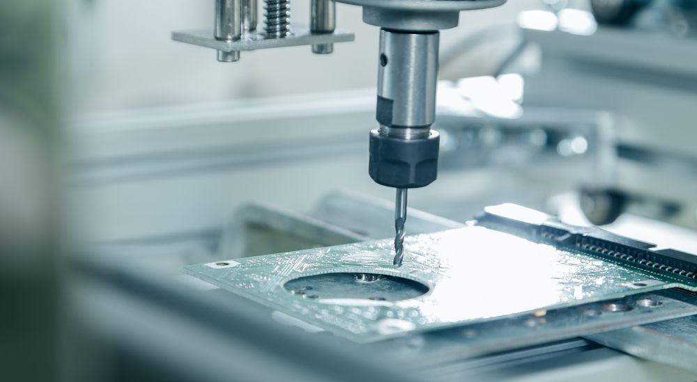
Design for Manufacturability (DFM) Considerations
Effective potting starts at the design stage. Component spacing, enclosure geometry, and venting paths all influence material flow and cure consistency. Avoid trapping air pockets under large components or within cavities. Design access points for dispensing and factor in material shrinkage during cure. Collaborating early with manufacturing teams helps align design intent to process capability and limits delays during production.
Potting vs. Conformal Coating
Potting and conformal coating both protect electronic assemblies, but their applications and strengths differ. Potting fully encapsulates components in a thick layer, offering mechanical reinforcement and environmental sealing. Conformal coating forms a thin, flexible film that guards against moisture and contamination without adding bulk. When weight, access, or serviceability are priorities, coating may be preferred. For rugged environments, potting provides more complete protection.
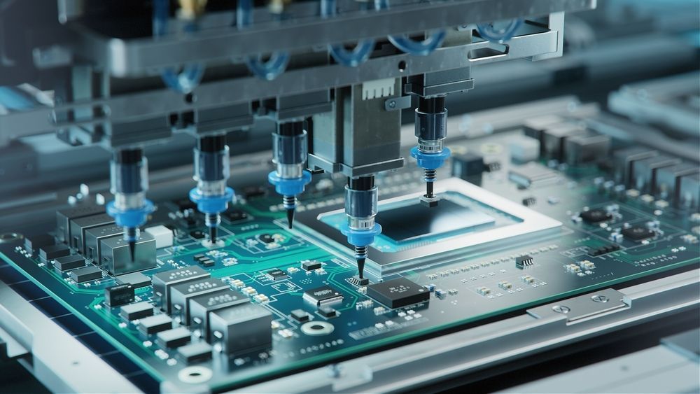
The Potting Process
Successful potting depends on process control, material handling, and environmental conditions. Each phase must be planned to avoid defects and preserve functional integrity.
Preparation
Before potting, the assembly must be cleaned, dried, and inspected. Any contaminants, including flux residue or moisture, can interfere with adhesion and curing. Fixtures or dams may be used to contain flow in open designs. Proper fixturing and preheating (if required) help manage viscosity and enhance coverage across complex geometries.
Mix Potting Material
Mixing accuracy is critical, especially for two-part compounds. Incorrect ratios or air entrapment can compromise performance and lead to soft spots or incomplete curing. Materials should be degassed when needed and handled according to technical datasheets. Automated mixing and dispensing systems reduce variability and strengthen consistency in both lab and production environments.
Application
The potting material is dispensed into the enclosure or directly onto the
PCB, depending on design. Controlled fill rates prevent overflow, voids, or pressure on delicate components. For assemblies with tight tolerances, multiple pours or staged applications may be used. Avoiding turbulence during fill helps prevent air inclusion that could impact electrical insulation or adhesion.
Curing
Curing conditions depend on the material used. Some compounds cure at room temperature, while others require elevated heat or multi-stage processes. Controlled cure cycles help reduce internal stress and create a uniform bond. Assemblies should remain stable throughout curing to prevent flow shifts or pooling that could interfere with connectors or housing fit.
Testing and Validation of Potted Assemblies
Potted assemblies require functional validation and inspection to verify material performance. Electrical testing checks continuity, isolation, and signal integrity. X-ray or ultrasound may be used to detect voids or incomplete fill. For regulated industries, validation often includes thermal cycling or moisture exposure to confirm that potting meets mechanical and environmental performance targets.
Automated test development for PCBs is often paired with these inspections to confirm reliability under real-world conditions.
Common Challenges in Potting & How to Overcome Them
Potting introduces challenges that impact yield and long-term performance. Addressing them early helps reduce rework and prevent field failures.
Air entrapment can cause insulation failure — use vacuum degassing or staged pouring.
Incomplete curing leads to soft spots — verify mix ratios and monitor temperature.
Overflow or leakage disrupts fit — design containment features and test flow paths.
Partnering with EI Microcircuits
We integrate potting into controlled manufacturing workflows tailored to high-reliability assemblies. Our experience spans a range of materials, curing profiles, and inspection methods that reduce risk and strengthen product reliability.
For assemblies exposed to mechanical, thermal, or chemical extremes,
contact us to explore how we can align the process with application requirements.
let's talk
EI Microcircuits is comprised of three production facilities totaling over 100,000 square feet of climate-controlled manufacturing, engineering and warehousing. We are ready to be the solution to your next project. Contact Us, Request a Quote or Schedule a Tour today!
Manufacturing plant 1
1651 Pohl Road
Mankato, MN 56001
P: 507.345.5786
Manufacturing plant 2
2011 Klein Street
St. Peter, MN 56082
P: 507.934.5722
manufacturing plant 3
69 Power Drive
Mankato, MN 56001
P: 507.386.9160
*Each facility is configured to support your production needs. While maintaining continuity with each other in equipment, training and process control, each facility offers its own specialty. All facilities share the same data center to allow for seamless manufacturing between locations.