What Are PCB Gold Fingers & Why Are They Important?
Every printed circuit board ends at an edge. In that boundary lies a precise connection point where one system hands off power or data to another. Those slim, gold-plated contacts, known as gold fingers, quietly carry the burden of reliable communication between assemblies. They may seem like a minor detail, yet they define how consistently a product performs over thousands of insertion cycles, environmental shifts, and operating hours.
In high-reliability electronics, gold fingers bridge mechanical and electrical domains, providing both conductivity and resilience. Understanding how they function and why their quality matters reveals just how much performance depends on details measured in microns.
Understanding PCB Gold Fingers
What Are PCB Gold Fingers?
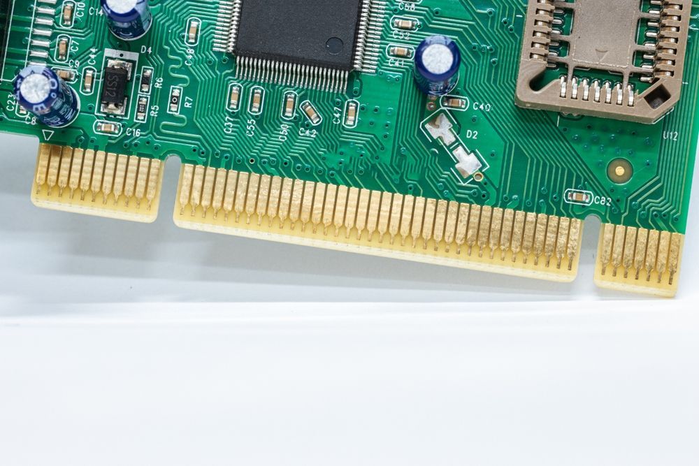
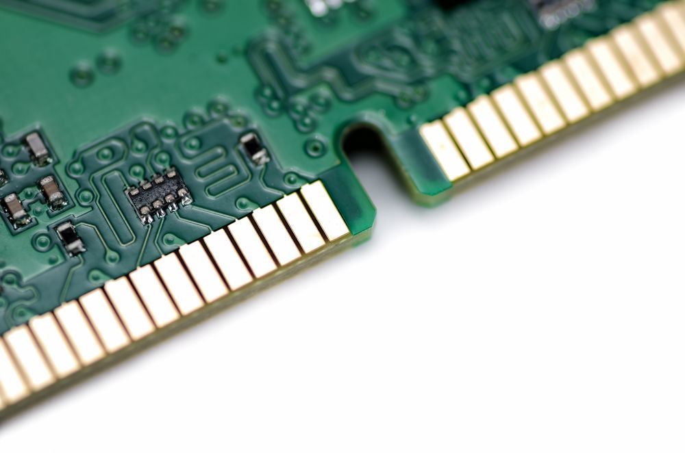
PCB gold fingers are gold-plated edge connectors located along the perimeter of a printed circuit board. They enable the board to mate with another PCB, backplane, or connector assembly, serving as the critical electrical interface between systems. These contact surfaces are typically plated with electroless nickel immersion gold (ENIG) or hard gold to achieve the right combination of conductivity, corrosion resistance, and wear durability.
The term “fingers” refers to their shape, narrow, evenly spaced pads that resemble the tines of a comb. Each pad acts as a conductive pathway, ensuring low-resistance signal transfer even under repeated mechanical stress.

Primary Functions
PCB gold fingers perform several essential roles in ensuring both electrical and mechanical reliability:
Electrical conduction: Provides a clean, low-resistance path for power and signal transmission.
Corrosion protection: Gold’s chemical stability prevents oxidation and degradation over time.
Wear resistance: Hard gold plating withstands repeated mating and demating cycles without losing integrity.
Dimensional precision: Maintains tight tolerances for alignment and contact pressure during insertion.
Together, these properties make gold fingers indispensable in systems that require dependable interconnection under variable environmental or operational conditions. Their quality directly influences signal fidelity, product longevity, and ultimately, the end user’s trust in the device.
The Importance of Gold Fingers in Mission-Critical Applications
In high-performance electronics, contact stability and surface integrity directly affect signal quality and system lifespan. For products that must perform flawlessly under vibration, temperature change, or frequent connection cycles, the choice of plating and process control around gold fingers is paramount.
Performance and Reliability Factors
The performance of PCB gold fingers is shaped by their ability to maintain consistent electrical contact and mechanical durability despite environmental and operational stress. They are engineered to resist:
- Temperature cycling, which can cause expansion, contraction, and microfractures.
- Vibration and mechanical shock, common in aerospace and industrial systems.
- Repeated insertion and removal, which gradually wears conventional plating.
- Corrosion and oxidation, which degrade conductivity over time.
Hard gold plating, with its controlled thickness and uniform grain structure, provides the balance of conductivity and abrasion resistance needed to meet these challenges. The process behind it (precise surface preparation, nickel underplating, and controlled gold deposition) ensures each contact point behaves predictably across the product’s life.
Applications Across Key Industries
Medical Devices
In
medical electronics,
gold fingers support modular connectivity in diagnostic equipment, imaging systems, and portable monitoring devices. Their corrosion resistance and biocompatibility help ensure signal accuracy and long-term reliability in regulated environments where field failure is not an option.
Aerospace and Defense
Aerospace
and
defense systems
depend on gold fingers for their ability to maintain low-resistance connections under vibration, altitude, and temperature extremes. Avionics modules, guidance controls, and radar systems all rely on stable contact performance where repair opportunities are limited, and reliability is mission-critical.
Industrial Automation
In
industrial control and robotics, gold fingers provide durable connections for replaceable modules and interface boards that see frequent maintenance. Their wear resistance and consistent electrical properties help prevent downtime in production environments where continuity is essential.
Technical Standards and Best Practices
Gold fingers occupy a small area of the printed circuit board, yet they are governed by some of the
most precise manufacturing standards in the electronics industry. These standards define how the plating is applied, how edges are beveled, and how the finished connector is inspected for uniformity and wear resistance. Consistent adherence to these guidelines ensures every contact performs reliably, even after thousands of insertion cycles.
Key Standards Guiding Gold Finger Manufacturing
Several industry standards shape the quality expectations for gold finger design and production:
- IPC-6012 outlines the qualification and performance requirements for rigid printed boards, including surface finishes and plating thickness.
- IPC-A-600 details acceptability criteria for PCB surface conditions and connector edges.
- IPC-4552 specifies requirements for electroless nickel immersion gold (ENIG) coatings, emphasizing corrosion protection and adhesion.
- MIL-G-45204 defines the composition and plating requirements for electrodeposited gold used in aerospace and defense applications.
These standards collectively ensure the plating is applied uniformly, bonded securely to the nickel underlayer, and capable of withstanding repeated use without degradation.

Best Practices in Gold Finger Design
Designing gold fingers requires attention to geometry, spacing, and process sequencing. Proper beveling at the insertion edge reduces wear on both the connector and mating surface. Solder mask clearance should be maintained to prevent contamination during plating and to ensure accurate contact alignment.
Controlling plating thickness is also essential. Hard gold layers are typically between 30 and 50 microinches thick, depending on the expected number of mating cycles and contact pressure. Uniform thickness prevents premature wear and minimizes resistance variation across the connector.
Before plating, surfaces must remain free from solder flux, oxidation, or handling residue. Even minor contamination can interfere with adhesion or conductivity. By maintaining clean, well-defined plating boundaries and following a disciplined inspection process, manufacturers achieve the consistency required for dependable long-term performance.
How EI Microcircuits Delivers Precision in Gold Finger Manufacturing
Producing reliable gold finger interfaces requires more than surface finish control. It depends on engineering discipline, manufacturing consistency, and verification at every stage of production. At EI Microcircuits, we manage all three through an integrated approach that unites design, process control, and quality assurance within one system.
Engineering Expertise
Our engineers evaluate each layout for manufacturability before production begins. Design-for-manufacturability reviews confirm that connector geometry, bevel angle, and plating clearance meet both IPC and customer-specific requirements. We also collaborate directly with OEM design teams to define the optimal gold thickness, ensuring each interface aligns with expected insertion frequency and environmental exposure. This early-stage support reduces variation and prevents downstream rework.
Manufacturing Excellence
EI Microcircuits maintains controlled plating processes to achieve uniform gold deposition and reliable adhesion to the nickel underlayer. Automated Optical Inspection (AOI) and X-ray verification confirm alignment, thickness, and surface integrity across every production lot. Our facilities support both electroless nickel immersion gold (ENIG) and hard gold finishes, applied through closely monitored parameters that ensure repeatable results.
Regulatory and Quality Commitment
All gold finger assemblies are built within
quality management systems that include ISO 13485 for medical devices and AS9100D for aerospace and defense. These systems govern traceability, inspection, and documentation throughout
the manufacturing process. From material qualification to final test, every gold-plated interface is verified to meet its intended electrical and mechanical performance.
Common Challenges with PCB Gold Fingers and How We Solve Them
Gold finger performance depends on precision at every manufacturing step. Small deviations in plating, surface preparation, or handling can lead to larger issues once the assembly enters service. At EI Microcircuits, our process controls and inspection protocols are designed to identify and eliminate these risks before they affect product quality.
Issues We Help Prevent
Common challenges in gold finger production include:
- Uneven plating thickness which can lead to inconsistent contact pressure and electrical resistance.
- Contamination or oxidation on copper surfaces before plating results in poor adhesion.
- Edge misalignment or over-beveling which affects fit and wear characteristics.
- Nickel underplating defects, causing delamination or brittle interfaces.
- Insufficient cleaning or handling control, which introduces oils or residues that interfere with conductivity.
- Each of these issues reduces connection reliability and can shorten the lifespan of the finished product.
Solutions We Provide
EI Microcircuits maintains strict environmental and process controls to prevent these defects. Our plating baths are regularly monitored for chemical balance and purity, ensuring consistent deposition across every lot. Surfaces are cleaned, masked, and inspected prior to plating to eliminate contaminants that could affect adhesion.
Post-plating, every board undergoes dimensional and visual inspection using high-resolution imaging systems to verify bevel quality, alignment, and uniformity. Gold thickness is measured and documented to confirm compliance with IPC and customer specifications.
Choosing the Right Partner for PCB Assemblies with Gold Fingers
Every engineer faces the same moment in a project, when a product’s success depends on the integrity of its smallest details. Gold fingers may seem minor, but they carry the responsibility of maintaining perfect communication between systems that cannot afford to fail. The challenge is ensuring that every plated edge performs the same way, every time, across the life of the product.
That responsibility belongs to those who design and deliver mission-ready technology. Your job is to ensure performance, compliance, and reliability under conditions that test every connection. Our job is to help you get there with confidence.
At EI Microcircuits, we’ve built our processes to support engineers like you. We guide teams through design-for-manufacturability reviews, controlled plating processes, and full-lifecycle verification so that every contact, every interface, and every board you produce meets its intended purpose.
Reach out to EI Microcircuits today and discuss how our expertise in PCB gold finger manufacturing and high-reliability assembly can strengthen the systems you’re building. We’ll help you turn complex requirements into proven results, because your success is the measure of ours.
let's talk
EI Microcircuits is comprised of three production facilities totaling over 100,000 square feet of climate-controlled manufacturing, engineering and warehousing. We are ready to be the solution to your next project. Contact Us, Request a Quote or Schedule a Tour today!
Manufacturing plant 1
1651 Pohl Road
Mankato, MN 56001
P: 507.345.5786
Manufacturing plant 2
2011 Klein Street
St. Peter, MN 56082
P: 507.934.5722
manufacturing plant 3
69 Power Drive
Mankato, MN 56001
P: 507.386.9160
*Each facility is configured to support your production needs. While maintaining continuity with each other in equipment, training and process control, each facility offers its own specialty. All facilities share the same data center to allow for seamless manufacturing between locations.


