Aluminum vs Copper PCBs: What to Know
Design decisions around
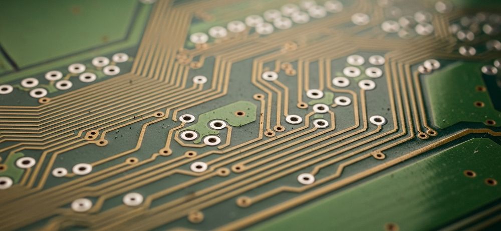
PCB materials often focus on electrical performance, but heat dissipation can be the limiting factor in reliability. It’s easy to assume all metal-core boards behave similarly, yet aluminum and copper substrates differ in more than just conductivity. These differences affect layout strategy, thermal limits, and long-term stability. In high-reliability builds, thermal control functions as a design constraint rather than a passive feature.
Material Properties and Thermal Performance
Copper and aluminum each bring distinct thermal and mechanical traits to PCB substrates. Copper has superior thermal conductivity, typically around 380 W/m·K, which helps transfer heat away from active components. Aluminum conducts heat at a lower rate, often between 150 and 230 W/m·K, but weighs less and costs less per unit.
These differences influence how heat spreads through the board and how layers are structured. Copper substrates handle tighter thermal tolerances and may reduce the need for additional heat sinks. Aluminum, while less conductive, still performs effectively in moderate-power applications.
Material choice affects operating temperatures, mechanical strength, expansion rates, and weight. These combined factors influence board layout and overall product performance.

Manufacturing Considerations
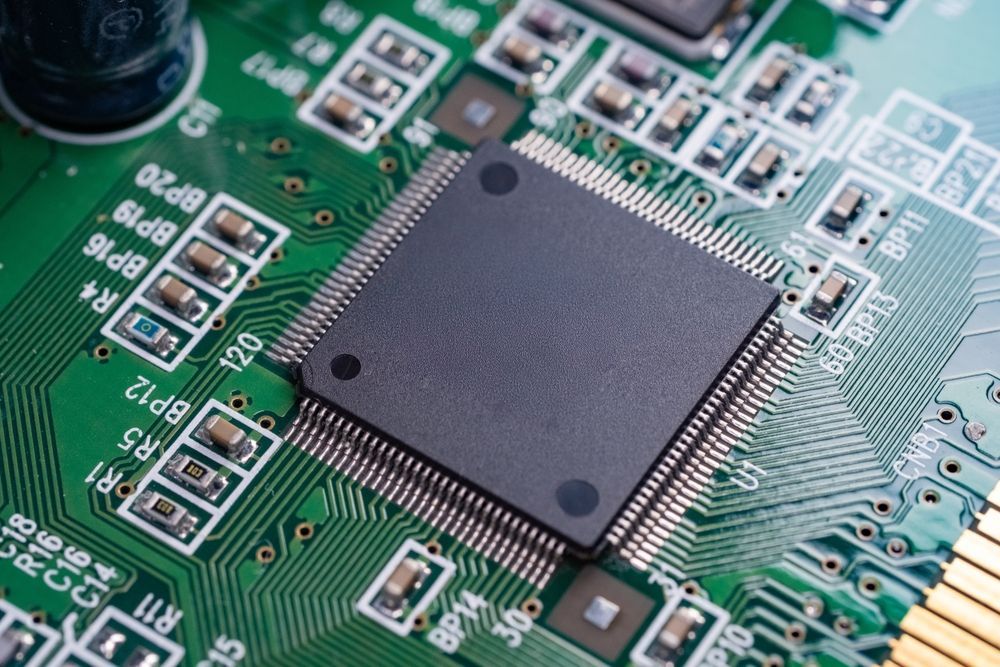
Material selection directly impacts both performance and manufacturability across multiple phases of production. Copper-core PCBs demand specialized drilling and routing equipment due to their hardness and thickness. Tool wear can increase, and tighter process control is often needed to maintain dimensional accuracy. Aluminum is easier to machine and offers more predictable behavior during fabrication, which can shorten lead times in some builds.
Thermal expansion is another factor. Copper’s low coefficient of thermal expansion makes it ideal for applications involving wide temperature ranges or mechanical stress. Aluminum expands more, but it may still be appropriate for less demanding environments.
These manufacturing variables should be evaluated alongside performance goals, especially in projects where turnaround time, yield, and process stability directly impact program success.
Application-Specific Use Cases
The functional demands of an end-use environment often shape PCB material decisions. Aluminum PCBs are commonly used where thermal control is needed, but cost, weight, or design simplicity take priority. Copper substrates accommodate more complex requirements and are suited for applications with high thermal loads or precise mechanical tolerances.
Common applications include:
- LED lighting systems where aluminum helps manage heat in compact enclosures
- Power supplies and converters for electronics that balance thermal needs and cost
- Automotive electronics, where lightweight, thermally efficient boards are preferred
- RF and microwave circuits that benefit from copper’s conductivity and dimensional stability
- Aerospace and defense systems, where copper’s strength and thermal consistency offer reliability
- Medical imaging equipment that operates under strict temperature and mechanical conditions
Key Selection Criteria for OEMs
Choosing between aluminum and copper substrates involves more than performance metrics. OEMs must weigh multiple factors tied to end-use requirements, regulatory expectations, and production goals. Each decision impacts reliability, cost structure, and manufacturability.
Key selection criteria include:
- Thermal load and heat spreading requirements based on component density and power levels
- Mechanical strength and rigidity are needed for handling, mounting, or vibration exposure
- Weight limitations in applications like aerospace or wearables
- Budget constraints and material availability in specific regions or programs
- Production volumes that influence tooling investments and fabrication time
- Industry-specific standards that guide material compatibility and process validation
Aligning these variables with design intent helps teams reduce rework, streamline execution, and meet long-term reliability targets.
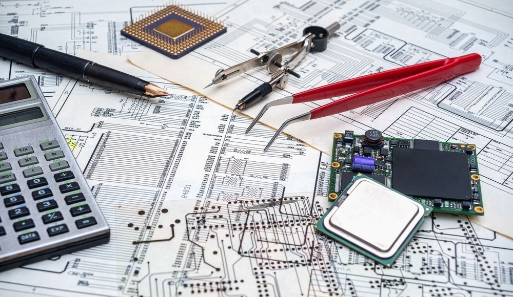
EI Microcircuits' Expertise in High-Reliability PCBA
Complex builds for regulated industries demand more than technical capability. They rely on disciplined processes, certified systems, and experienced teams. Our approach reinforces long-term stability for the
sectors we partner with, grounded in a proven framework for traceability and process control.
Materials-Driven DFM Support
Design for manufacturability begins at the material level. At EI Microcircuits, we evaluate how copper and aluminum substrates influence thermal modeling, trace routing, and stackup design. Our engineering team works directly with customers during layout development to recommend pad sizing, via placement, and thermal relief structures that align with manufacturing constraints.
Each recommendation supports yield, consistency, and solder joint reliability over time. Input is grounded in design intent and validated against production experience. These decisions reduce rework and enhance reliability in the final product.
This early engagement model equips OEMs to enter production with confidence, especially in projects where thermal limits and material behavior directly affect function and form.
Robust Manufacturing Capabilities
We build for reliability in industries that do not tolerate variation. Our SMT lines accommodate a wide range of board thicknesses, surface finishes, and component densities. Both copper and aluminum builds are handled using tailored settings that reflect material-specific behaviors during soldering and reflow.
Maintaining dimensional control, placement accuracy, and solder quality all require disciplined execution. Our teams monitor key process indicators in real time to catch deviations early and preserve traceability from lot to lot.
Manufacturing is governed by IPC class certifications, which guide quality expectations across the full production cycle. These standards support programs where process reliability and product durability are required from first build through end of life.
Industry-Specific Compliance and Process Control
We maintain certifications such as ISO 13485, AS9100D, and ITAR registration to meet the expectations of the sectors we partner with. These systems shape how we document, audit, and validate each build. Material selection, solder alloy compatibility, and thermal performance are reviewed during pre-production to confirm alignment with customer and regulatory requirements.
Every assembly is subject to serialized traceability, incoming inspection, and closed-loop quality tracking. This structure supports repeatable outcomes across both standard and thermally demanding builds.
Surface-mount technology (SMT) is central to our process flow and is supported through automated optical inspection, X-ray validation, and functional test protocols. These systems enable long-term performance in industries where consistency matters over the full product lifecycle.
Integrated Services for Turnkey Outcomes
EI Microcircuits delivers electronics manufacturing services (EMS) that integrate material expertise, process control, and functional validation into a single workflow. We support box build assemblies, complex PCB stackups, and component-level integration under one roof. PCB inspections are built into each stage of production, from first article to final packaging, using AOI, X-ray, and electrical test.
We also develop
automated test solutions for PCBs, tailored to specific performance thresholds and compliance requirements. These services help OEMs reduce risk and extend product life through predictable, high-reliability output.
To learn how our EMS model fits your technical goals,
contact us today to start a conversation.
let's talk
EI Microcircuits is comprised of three production facilities totaling over 100,000 square feet of climate-controlled manufacturing, engineering and warehousing. We are ready to be the solution to your next project. Contact Us, Request a Quote or Schedule a Tour today!
Manufacturing plant 1
1651 Pohl Road
Mankato, MN 56001
P: 507.345.5786
Manufacturing plant 2
2011 Klein Street
St. Peter, MN 56082
P: 507.934.5722
manufacturing plant 3
69 Power Drive
Mankato, MN 56001
P: 507.386.9160
*Each facility is configured to support your production needs. While maintaining continuity with each other in equipment, training and process control, each facility offers its own specialty. All facilities share the same data center to allow for seamless manufacturing between locations.